Products & Technologies
Products & Services
Company
Contact
Products & Services
Products & Technologies
Services
Resources
Company
Contact
Applied Vericell™ Solar Wafer Inspection System
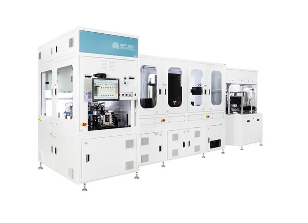
The Applied Vericell Solar Wafer Inspection system is the industry’s most advanced fully automated bare wafer inspection tool for crystalline silicon PV wafer and cell production. The Vericell system’s multiple integrated inspection modules automatically evaluate each wafer to find and eliminate defective wafers from production, resulting in significant manufacturing savings. It measures and reports on a wide range of parameters including wafer thickness, thickness variations, warpage and resistivity. The Vericell system also detects defects including saw marks, chipped edges, damaged chamfers, stains, pin holes and micro-cracks.
Through the use of state-of-the-art photoluminescence (PL) technology, the Vericell system can detect oxygen circle to increase cell line yield. By removing oxygen circle wafers, Vericell customers can achieve overall improvement in their factory’s average cell efficiency yield and increase factory profitability. In addition, the Vericell system delivers the lowest breakage rate in the industry with the highest inspection throughput of up to 16,000 wafers per hour.
Vericell provides three types of equipment for full, half and rectangular wafer sizes used in the solar wafer and cell industry.
- Inspection equipment for silicon wafer factory
- IQC sampling inspection of cell factory
- On-line 100% inspection of cell factory
Key features of Vericell:
- Detect wafer size, thickness, warpage, surface edge chip, side edge chip, chamfer edge chip, saw mark, resistivity, stain, TTV, μcrack, pinhole and carrier lifetime
- Available for dual lanes half cut wafer (throughput 24,000 wafers per hour), whole wafer (throughput 16,000 wafers per hour)
- Super thin wafer thickness ≥90μm
- Integrated AI and deep learning to maximize the detection rate
- Supports coin stack, cassette loading and unloading
- Available for connection of MES system
- Can support RFID hierarchical management connect equipment systems
- Mobile app monitors the equipment status and statistical data in real time
- Small footprint provides maximum speed and throughput
- First tool to inspect the G12 wafer
The Vericell Solar Wafer Inspection System combines high productivity with unique advanced inspection techniques that meet SEMI® solar standards to optimize the entire manufacturing line.