Products & Technologies
Products & Services
Company
Contact
Products & Services
Products & Technologies
Services
Resources
Company
Contact
Solar
Solar
Technology
Specialties
Printed Electronics
Fine Line / Wrap Around Electrodes
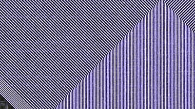
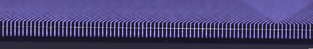
The accuracy and precision of Applied Materials equipment make possible with screen-printing processes usually achievable only through subtractive photolithographic techniques.
Thanks to the continuous focus on research and development, Applied can provide proprietary processes to accomplish the ultimate industry challenges, such as:
- Fine line Printing down to 15 μm and line/space down to 30/30 μm
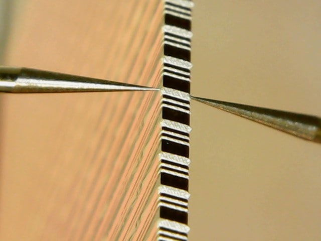
- Wrap Around Electrodes, or Side Wiring, entirely performed by screen printing
- Conductive traces for medical sensors
- Honey-comb metal structures for indium tin oxide (ITO) replacement
- Antennas for consumer electronics and white goods
The fine line printing process has been optimized for several materials, mainly silver and copper-based (e.g., micro, nano-inks, and reactive inks).
The so-called wrap-around electrode, or side wiring, is an Applied proprietary process explicitly developed for seamless tile-based microLED displays: this process allows to fully print around a substrate edge, thus enabling conduction from the top to the bottom of the substrate itself.
For more details, contact us at printed_electronics@amat.com