Advanced Substrates
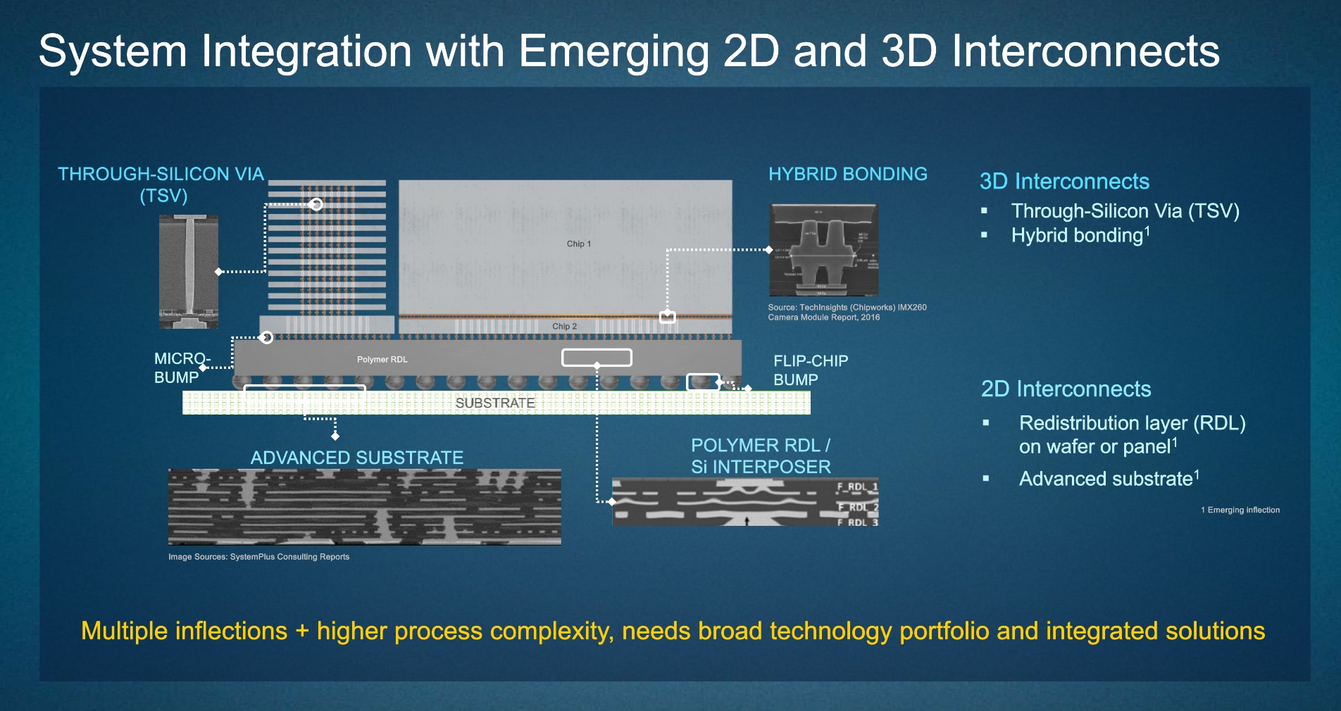
As more and more chiplets are integrated into a single package, those packages must be larger and more sophisticated. As packages grow, the use of 300mm wafers creates limitations since only a few large packages can fit into the wafer format. There is a need to port high-density, wafer-level interconnect technologies onto larger substrates. The industry is looking to new rectangular substrates with larger dimensions of up to 600mm x 600mm.

Applied Materials is working to accelerate the ecosystem for large semiconductor-grade advanced substrates based on a variety of materials. These new substrates will enable designers to use larger packages and integrate more chips at a competitive cost. This comes with added complexity in process flow and control.
To be successful, customers need front end-level cleanliness, process control and metrology along with a cost of ownership that is compatible with packaging applications. With years of experience depositing wiring on substrates as large as 600 by 600 millimeters, Applied Materials’ Topaz PVD tools integrate multiple process steps in a high-throughput cluster architecture and can deposit films on both sides of each panel. The Topaz tools complement our strength in metals deposition, display and metrology, which are all technologies that are necessary to enable panel-level substrates.
With decades of experience engineering large substrates for the display industry and e-beam technology that can see through the layers of the materials, Applied Materials offers customers access to non-destructive methods to test designs and ensure quality. Applied is working broadly with our customers and partners to accelerate the heterogeneous integration ecosystem including panel processing.
More information can be found on our Master Class and blogs on this topic.
