Products & Technologies
Products & Services
Contact
Products & Services
Products & Technologies
Services
Resources
Contact
Posted
September 07, 2021

Stay updated on our content.
The Fourth Era of Computing Needs More than Advanced Logic and Memory Chips

Sep 08, 2021
Applied Materials today held its third Master Class of the year, focusing on two important and fast-growing areas of the semiconductor industry: ICAPS and advanced packaging. ICAPS stands for IoT, Communications, Automotive, Power and Sensors. ICAPS encompasses all but the three most advanced nodes in foundry-logic. Advanced packaging is about heterogeneous design, which is increasingly being adopted by semiconductor and systems companies to drive their power, performance, area/cost and time-to-market (PPACt™) roadmaps as classic Moore’s Law 2D scaling slows.
Why we’re featuring these topics in the same event may not seem obvious. What ICAPS and advanced packaging have in common, however, is a highly enabling role in the fourth era of computing—which is now upon us and driving unprecedented demand for silicon and equipment. Allow me to explain.
Into the Fourth Era of Computing
In 2018, machines generated more data than humans for the first time. We believe this milestone marks the beginning of the fourth era of computing whereby the Internet of Things (IoT), Big Data and AI are creating a new wave of growth for the semiconductor industry, complementing the markets for PCs and smartphones which defined the second and third computing eras (see Figure 1). By 2025, we expect machines to generate 99 percent of the data created each year.
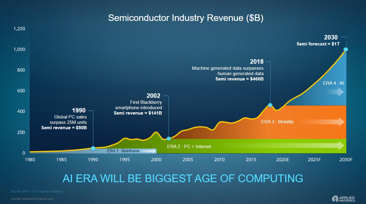
Figure 1: 2018 marked the beginning of the fourth era of computing, where the Internet of Things, Big Data and AI are creating a new wave of growth for semiconductors.
Most of this data will come from the billions of IoT products on the network edge, in applications ranging from farming to factory automation—and from healthcare to home security. ICAPS devices such as CMOS image sensors, MEMS devices, RF chips, power devices and analog-to-digital converters define how these IoT products function and interact with the physical world. Using a biological metaphor described in an earlier blog by my colleague, Dr. Mike Chudzik, ICAPS provides computers with eyes, ears—even noses and skin—so they can sense the world, generate information and communicate over the airwaves. Per the same analogy, cloud data centers are like the brains of this distributed system. And who is to say the brains are more important? After all, around 70 percent of a smartphone’s semiconductor content is ICAPS chips, and without them the device is hardly more useful than a calculator. Without ICAPS, there can be no autonomous vehicles.
Bringing Technology Solutions to Vertical Markets
Another thing that may not seem obvious is why ICAPS and advanced packaging are nested within the same business unit at Applied Materials. The reason is that the end markets—such as high-performance computing, wireless communications, automotive, power distribution and digital imaging—are unique and highly specialized, both from a market perspective and from a materials engineering perspective. Applied’s ICAPS and packaging teams include device experts who can relate to the customers and their unique roadmap challenges. They have the ability to cut across Applied’s broad and deep portfolio of materials engineering technologies, including co-optimized and integrated solutions, to enable vertical market breakthroughs.
IMS for CIS
One example Mike shared in the Master Class is using co-optimization and Integrated Materials Solutions (IMS™) to improve CMOS image sensors (see Figure 2). Our dedicated CIS engineering team has designed an integrated platform solution that is in qualification at customer sites to improve next-generation digital cameras in the areas of resolution, light sensitivity and dynamic range.
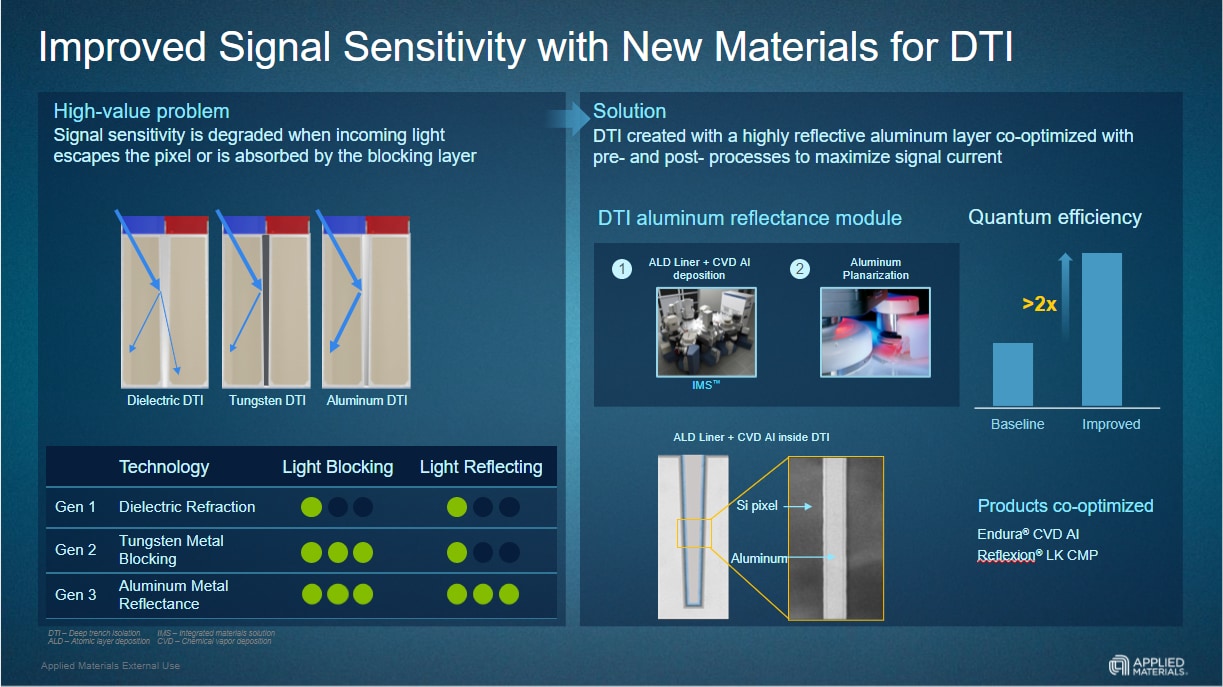
Figure 2: In CMOS image sensors, Applied is using materials engineering to improve photo signals and increase pixel density at the same time by minimizing electrical and optical crosstalk between neighboring photodiodes.
Materials Engineering for Power Devices
Silicon carbide (SiC) is the “silicon superhero” powering today’s most advanced electric vehicles, giving them unprecedented torque and range. Scaling silicon carbide from 150mm wafers to 200mm wafers will help grow the market by reducing cost and boosting output. A key challenge is that SiC is harder than silicon but also susceptible to crystal lattice damage that degrades device performance, wastes power and generates heat.
Device experts from our ICAPS team have partnered with our equipment businesses to create unique systems that are highly optimized to the needs of leading chipmakers. Today we introduced a new SiC-optimized CMP system that perfectly planarizes raw silicon wafers to enable defect-free epi layers to be formed. We also launched a “hot implant” technology that allows ions to be precisely implanted and diffused into the silicon carbide crystal while preserving the integrity of the lattice (see Figure 3).
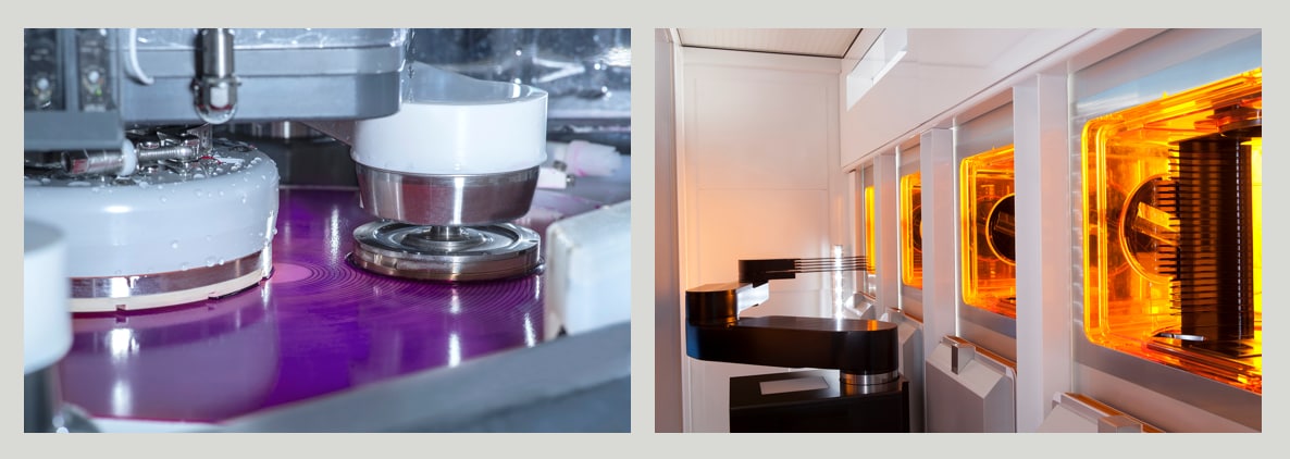
Figure 3: Applied’s new silicon carbide-optimized Mirra® Durum™ CMP system (left) and VIISta® 900 3D hot ion implant system (right) are specially designed to help enable the SiC chip industry’s move to larger, 200mm wafers.
These are just two of dozens of programs that will bring the breadth and depth of Applied Materials to highly specialized ICAPS devices and markets.
ICAPS and Advanced Packaging: Enabling a Virtuous Cycle
In the fourth era of computing, billions of new ICAPS devices at the edge are driving exponential growth in data generation which needs to be processed in the cloud.
At the same time, as another of my colleagues Dr. Nirmalya Maity explained in a recent blog, the slowing of classic Moore’s Law 2D scaling is making it harder for chipmakers to place all of the transistors they need for high-performance computing, machine learning and inferencing on a single die. This is why heterogeneous design and integration are becoming so important to the world’s leading chip and systems companies: it gives them the flexibility to disaggregate designs for area/cost savings while integrating them on advanced packages to optimize power and performance. This newfound flexibility—along with the opportunity for silicon IP reuse—also promises faster time to market. In short, heterogeneous design and advanced packaging enables PPACt.
In keeping with our goal to be the PPACt enablement company for our customers, Applied today made several advanced packaging announcements.
Die-to-Wafer Hybrid Bonding: Today, we are building on our collaboration with BE Semiconductor Industries N.V. (Besi) to provide customers with a proven, co-optimized equipment solution for die-based hybrid bonding. In addition, we’re helping our customers by offering advanced software modeling and simulation capabilities for hybrid bonding, along with the ability to produce test vehicles. All of this capability is available under one roof, at our Advanced Packaging Development Center in Singapore, where we are already collaborating with customers.
Wafer-to-Wafer Hybrid Bonding: Today we announced another joint development agreement, with EV Group (EVG), aimed at providing co-optimized manufacturing solutions for wafer-to-wafer hybrid bonding. The collaboration brings together Applied’s expertise in deposition, planarization, implant, metrology and inspection with EVG’s leadership in wafer bonding, wafer pre-treatment and activation, as well as alignment and bond overlay metrology.
Larger Advanced Substrates: Today we also announced the recent acquisition of Tango Systems and our plans to enable customers to go far beyond the area constraints of 300mm silicon wafer substrates. Customers will be able to design larger advanced packages manufactured on rectangular substrates of up to 600mm x 600mm with fine-pitch interconnects (see Figure 4). Applied is also enabling its customers to use technologies from its display business such as eBeam review.
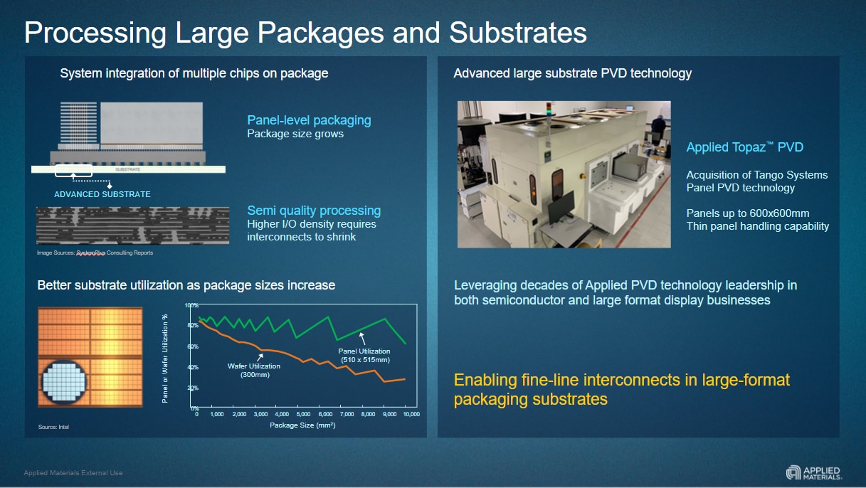
Figure 4: To enable larger package sizes with greater interconnect density, Applied is offering state-of-the-art panel-level processing technology from its recent acquisition of Tango Systems.
In summary, the AI Era is fueling growth from the edge to the cloud. To enable this growth era, the industry needs simultaneous innovation across leading edge, ICAPS and advanced packaging technologies. The end result is a virtuous cycle of data generation and AI processing that will unlock trillions of dollars in economic value.
Tags: AI Era, Moore's Law, ICAPS, PPACt, iot, communications, automotive, power, sensors, silicon carbide, CIS, CMP, implant, packaging, hybrid bonding, Heterogeneous Design, heterogeneous integration, chiplets, advanced substrates, Tango
Sundar Ramamurthy, Ph.D.
Wafer-Level Packaging, Specialty Semiconductors and Epitaxy Markets

Dr. Sundar Ramamurthy is responsible for Applied’s business in wafer-level packaging, specialty semiconductors and epitaxy markets. In his role, Sundar leads an integrated team across the company to fuel growth in some of the fastest growing markets in the semiconductor industry. He has led teams that commercialized 20+ new products to solve critical transistor and interconnect scaling challenges by introducing new materials and interface engineering solutions into volume manufacturing. Sundar holds a Ph.D. in materials science and engineering from the University of Minnesota. He has more than 30 patents granted or pending. Sundar is also an active mentor with the Miller Center in Santa Clara University for accelerating social enterprises.

Adding Sustainability to the Definition of Fab Performance
To enable a more sustainable semiconductor industry, new fabs must be designed to maximize output while reducing energy consumption and emissions. In this blog post, I examine Applied Materials’ efforts to drive fab sustainability through the process equipment we develop for chipmakers. It all starts with an evolution in the mindset of how these systems are designed.
Innovations in eBeam Metrology Enable a New Playbook for Patterning Control
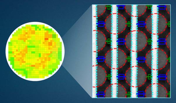
The patterning challenges of today’s most advanced logic and memory chips can be solved with a new playbook that takes the industry from optical target-based approximation to actual, on-device measurements; limited statistical sampling to massive, across-wafer sampling; and single-layer patterning control to integrative multi-layer control. Applied’s new PROVision® 3E system is designed to enable this new playbook.
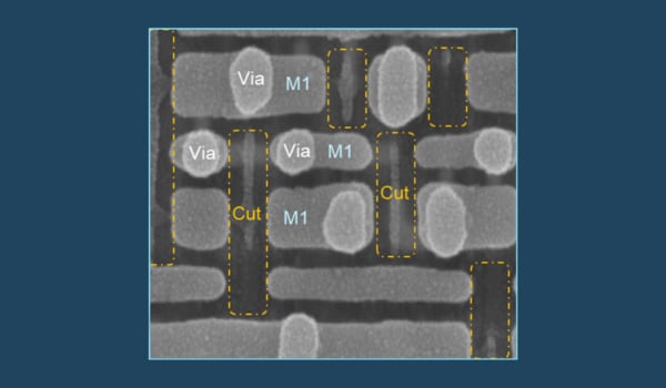
Breakthrough in Metrology Needed for Patterning Advanced Logic and Memory Chips
As the semiconductor industry increasingly moves from simple 2D chip designs to complex 3D designs based on multipatterning and EUV, patterning control has reached an inflection point. The optical overlay tools and techniques the semiconductor industry traditionally used to reduce errors are simply not precise enough for today’s leading-edge logic and memory chips.