Products & Technologies
Products & Services
Contact
Products & Services
Products & Technologies
Services
Resources
Contact
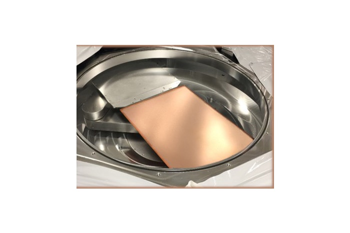
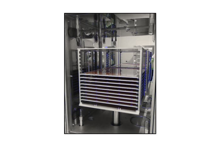
Topaz™ PVD
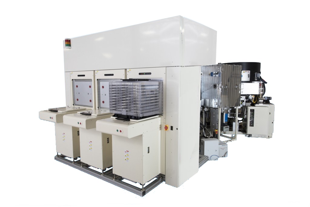
The Applied Topaz PVD system serves the growing market for PLP, demonstrating leading-edge capabilities on substrates of up to 600mm x 600mm. The demand for lower cost and higher performance electronics is motivating the industry to transition from WLP to PLP. Normalized capital costs for PLP are less than half that of wafer-level formats.
Process technologies and equipment developed for fan-out WLP, LCD, and printed circuit board have converged to make fan-out technology very affordable. Lower costs will enable this technology to proliferate to a variety of semiconductor packaging applications for mobile electronics (e.g., system-in-package, processors, RF, and power management), automotive, and Internet of Things.
In addition to PLP, the Topaz system addresses such applications as glass and organic interposers, and embedded die in substrate. Its unique modular architecture enables low contact resistance; double the minimum required adhesion strength; low stress; a cooler substrate temperature (<120C°); and a conformal seed layer with excellent sidewall coverage in etched or laser-drilled vias.
- 1 / 2
- 2 / 2