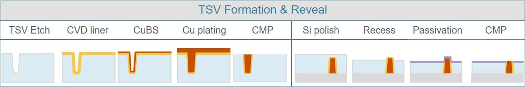
Through Silicon Vias (TSV)

Through Silicon Vias (TSV)

TSVs are vertical wires used to precisely connect stacked chips. They are formed by etching trenches into silicon and then filling them with insulating liners and metal wires.  

TSVs provide a means to improve the performance, functionality, and density of integrated circuits (ICs) by enabling high-speed communication between various components within a chip or between stacked chips. Using TSVs rather than bump-to-PCB connections allows designers to achieve improvements in performance of approximately 100X and reduce power consumption by approximately 15X depending on architecture and workload.

TSV fabrication can fall into three methods depending on how the via is constructed—via-first, via-middle and via-last. For example, the via-first process involves creating a deep via in the silicon from the top of the wafer followed by a reveal process that exposes the backside of the wafer. These vias can be a few microns in diameter and are very large and have high aspect ratios compared to the other features of integrated circuits. They need longer processing times and the fabrication process is quite complex.

The TSV process relies on a broad set of technologies from Applied Materials including dielectrics deposition, metals deposition, electroplating, chemical mechanical planarization (CMP) and etch. Pushing aspect ratios and productivity even further are Applied Materials’ Producer® InVia® 2, Endura® Ventura® 2 and Producer® Avila® systems, to help chipmakers achieve their integration, performance, and power goals.

More information on TSVs can be found on our Master Class and blogs on this topic.

TSV formation_reveal