첨단 기판
단일 패키지에 점점 더 많은 칩렛이 집적됨에 따라, 패키지는 더 크고 정교해야 합니다. 패키지가 더 커지면 웨이퍼 형태에는 몇 개의 큰 패키지만 들어갈 수 있기 때문에 300mm 웨이퍼 사용에 한계가 있습니다. 따라서 웨이퍼 수준의 고밀도 인터커넥트 기술을 더 큰 기판에 구현할 수 있는 방법을 찾아야 합니다. 업계에서는 최대 600mm x 600mm에 이르는 더 큰 치수의 새로운 사각 기판에 시선을 돌리고 있습니다.
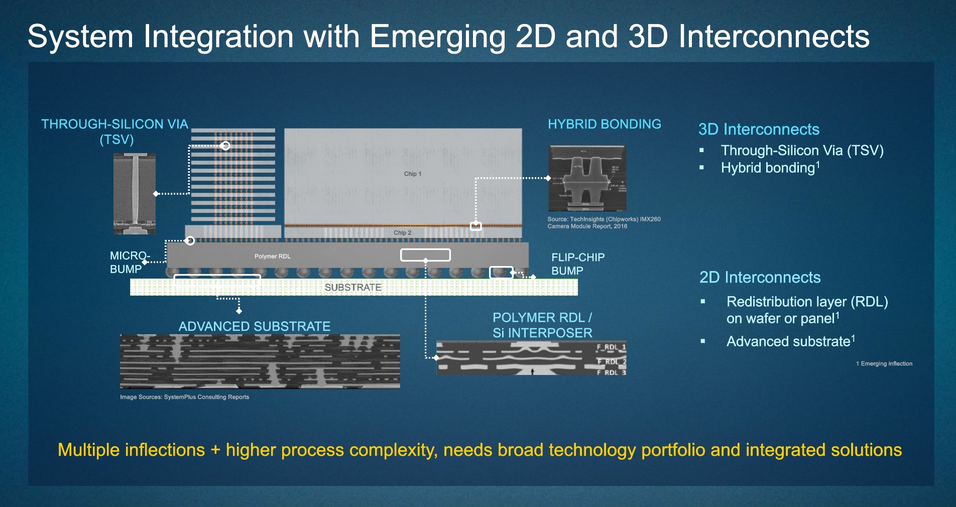
어플라이드 머티어리얼즈는 다양한 재료를 기반으로 대형 반도체급 첨단 기판을 위한 생태계를 가속화하기 위해 노력하고 있습니다. 이러한 새로운 기판을 통해 설계자는 경쟁력 있는 비용으로 더 큰 패키지를 사용하고 더 많은 칩을 집적할 수 있습니다.
고객의 성공을 위해서는 패키징 애플리케이션과 호환되는 소유 비용과 함께 전공정 수준의 청정도, 공정 제어 및 계측이 필요합니다. 수년간 600mm x 600mm의 대형 기판에 배선을 증착한 경험으로, 어플라이드 머티어리얼즈의 Topaz PVD 장비는 고 생산능력 클러스터 구조에 여러 공정 단계를 통합하고 각 패널의 양면에 필름을 증착할 수 있습니다. Topaz 장비는 패널 수준의 기판을 구현하는 데 필요한 기술인 금속 증착, 디스플레이 및 계측에서 강점을 보완합니다.
어플라이드 머티어리얼즈는 수십 년간 디스플레이 산업을 위해 대형 기판을 엔지니어링한 경험과 재료 내 여러 층을 투시할 수 있는 전자빔 기술을 통해, 고객에게 설계 테스트 및 품질 보장에 대한 비파괴 검사를 제공합니다.