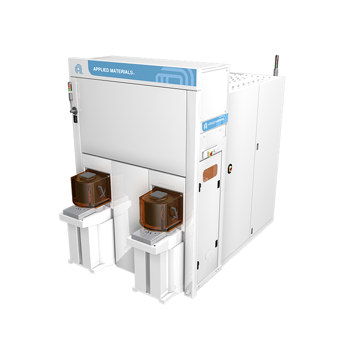
PROVision 4E eBeam Metrology
As advanced semiconductor technologies are undergoing rapid transformation, device architectures scale and pattern complexity increases driving the need for tighter process windows and greater sensitivity to pattern variability and marginal defectivity. The ICAPS semiconductor segment – IoT, communications, automotive, power, and sensors – faces similar transformation, driven by demand for reliable and specialized chips manufactured with stringent process control.
The PROVision™ 4E system delivers a design-based metrology approach tailored for manufacturing environments requiring high sampling density and layout-aware process control, spanning mature nodes and extending into advanced logic and memory technologies. It enables massive sampling and characterization of layout-sensitive hotspots, addressing both intra-die and die-to-die variability, which are increasingly critical in advanced FinFET logic nodes and next-generation DRAM architectures.
By leveraging contour-based layout analysis and generating millions of data points, the PROVision 4E provides granular, actionable insights into process uniformity and marginal defectivity, accelerating yield ramp and improving reliability across a broad range of technology nodes, from ICAPS devices to advanced logic and memory. Its high accelerating voltage combined with efficient back-scattered electron and secondary electron signal collection enables simultaneous CD and overlay measurements from a single image, facilitating comprehensive edge placement error characterization and rapid, step-specific root-cause analysis for both planar and 3D device architectures.
The PROVision 4E system empowers manufacturers to achieve tighter process control, faster R&D-to-high volume manufacturing (HVM) transitions, and proactive elimination of reliability risks. PROVision 4E is the latest-generation thermal field emission (TFE) eBeam system, optimized for massive SEM metrology and all-in-one edge placement error characterization, delivering high sampling density and layout-aware insight across a broad range of applications. It complements the PROVision 10 system which provides higher resolution and deeper penetration capability, with a cost-effective solution where sub-nanometer resolution and deeper penetration are not required.
- 1 / 3
- 2 / 3
- 3 / 3