製品・サービス
製品・サービス
Patterning
Patterning has enabled many generations of 2D scaling. In the past, patterning relied on a series of relatively straightforward optical masks and photolithography steps to print patterns, guiding subsequent materials removal and deposition steps. More recently, advances in photolithography have not kept pace with advances in chip design. Patterning approaches have shifted from lithography-reliant bidirectional to unidirectional, with the number of deposition and etch steps increasing significantly.
Even as the next EUV generation of lithography enters the roadmap, chipmakers are taking advantage of cost-effective, self-aligned multipatterning techniques, using pitch multiplication to create two or four lines from a single lithography pass. With or without EUV, edge placement error is a challenge that chipmakers must overcome to correctly align the features in one layer with the complementary features in the next. Materials engineering can play an enabling role, offering wider landing zones that can tolerate alignment variances that would otherwise adversely impact yields.
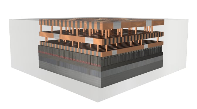
As the cost of lithography has increased, memory designers have taken to building 3D devices whereby cost reductions come not from 2D bit scaling, but 3D bit stacking. Costs are reduced by increasing bits per cubic millimeter instead of bits per square millimeter.
The animations below illustrate some of the challenges encountered and
state‑of‑the‑art patterning techniques used in creating today’s leading‑edge devices.
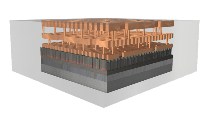
Patterning Technologies and Device Scaling
As we progress from 14 to 7nm devices and beyond, SADP and SAQP will be required for some layers and LE with either 193i or EUV lithography for others.
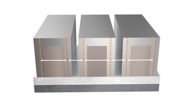
Pitchwalking
Pitchwalking refers to pitch variation between features; it can degrade performance, power efficiency, or signal integrity.
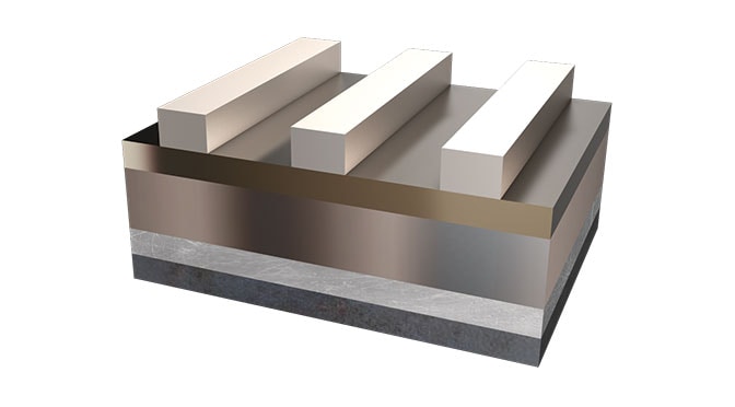
SAQP eases
litho resolution
Self-aligned quadruple patterning effectively decreases the lithography resolution by 4x using a spacer-based patterning approach with one lithography step and two spacer depositions.
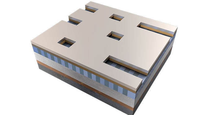
Multiple litho/etch creates
high‑density cuts and vias
To cut lines and create vias at densities too high to achieve in one pass, several iterations of lithography and etch are used.
Multi-color patterning
minimizes edge placement error
Multi-color patterning is a materials-based approach that minimizes EPE, which is the undesirable movement of an edge in any direction, resulting in shorts, opens, and reduced reliability.
Summary
Self-Aligned Multi-Patterning and materials engineering will be major contributors to minimizing EPE, the most critical factor limiting scaling. In the future, 80% of the patterning market will depend on materials‑enabled solutions.
With our breadth and depth of capabilities in materials engineering, Applied Materials systems can address the variations leading to pitchwalking and EPE, thereby enabling the fabrication of the semiconductor industry’s most advanced devices.