Products & Technologies
Products & Services
Company
Contact
Products & Services
Products & Technologies
Services
Resources
Company
Contact
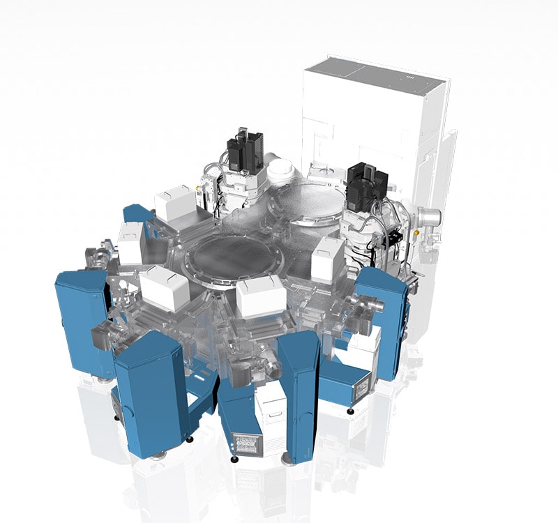
Endura® Ioniq™ W PVD
As integrated circuits and their components continue to scale downward, the dimensions of metal interconnects and contacts between components are also shrinking. One result is that the resistance in these connections is increasing.
The slowing effect produced by this higher resistance is typically referred to as resistance-capacitance delay (or RC delay) and affects chip performance by degrading speed and increasing power consumption. To create more compact and faster electronic devices, the resistance of these connections must be minimized to enable sustained scaling.
In a pioneering manufacturing combination with CVD and pre-treatment chambers on one high-vacuum platform, the new Applied Endura Ioniq PVD system is an Integrated Materials Solution™ that makes possible the metallization of pure tungsten (W) in a variety of contact applications. It replaces the high-resistivity, multi-tool combination of a titanium-nitride liner, a W nucleation layer, and a bulk W fill with a single PVD W layer integrated with bulk CVD W fill. Enhanced ionization and directional flux control in the Ioniq PVD chamber create excellent, uniform step coverage of a pure W film that serves as a low-resistance barrier and liner. The continuous high-vacuum environment preserves film integrity, further enhancing the purity and electrical conductance at the metallic interfaces.
As a scaling enabler, the Applied Endura Ioniq PVD system extends the use of W in critical contacts in logic applications below 5nm, while also providing a unique approach to metallize low-resistance connections in DRAM and NAND devices.