Products & Technologies
Products & Services
Company
Contact
Products & Services
Products & Technologies
Services
Resources
Company
Contact
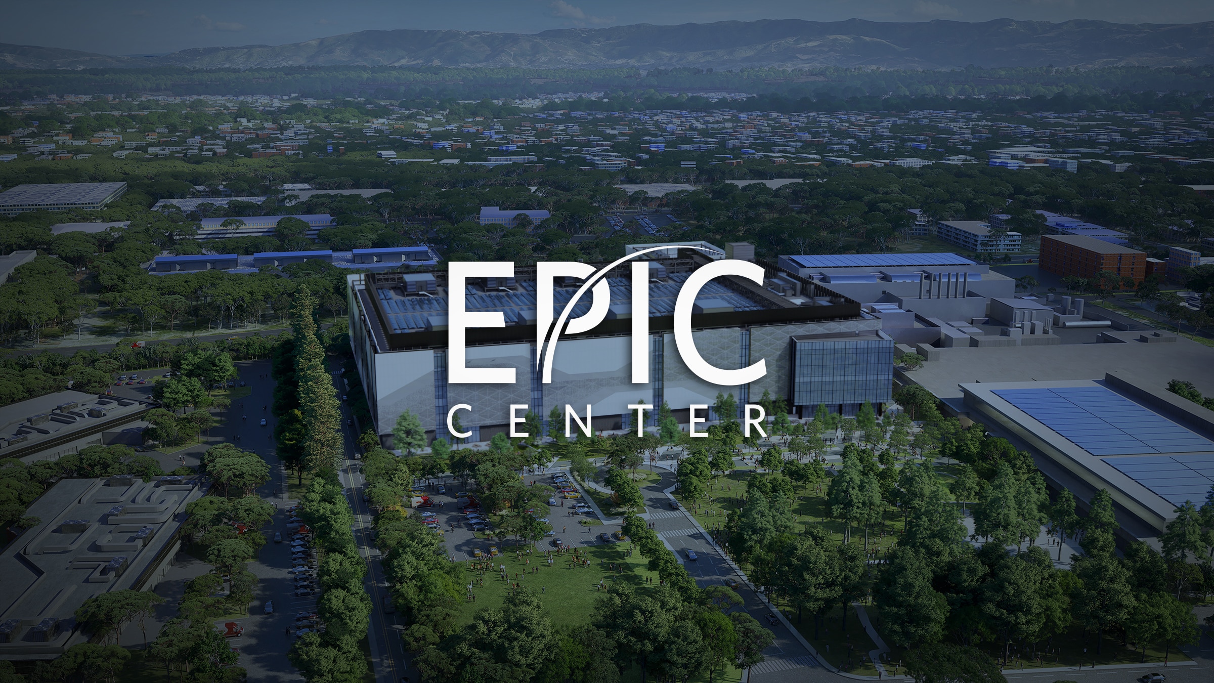
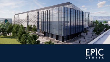
On May 22, 2023, Applied Materials announced a landmark investment to build the world’s largest and most advanced facility for collaborative semiconductor process technology and manufacturing equipment R&D at an Applied campus in Silicon Valley.
The Equipment and Process Innovation and Commercialization (EPIC) Center Silicon Valley is planned as the heart of a high-velocity innovation platform designed to accelerate development and commercialization of the foundational technologies needed by the global semiconductor and computing industries.
Applied’s EPIC Center in Silicon Valley represents the largest-ever U.S. investment in advanced semiconductor equipment R&D and is designed from the ground up to dramatically reduce the time it takes to commercialize breakthrough technologies from early-stage research to full-scale manufacturing. It does this by increasing speed, accuracy and efficiency through tighter collaboration and faster cycles of learning.
The EPIC Center Silicon Valley will open in 2026.
Learn more about Applied’s EPIC Platform for innovation.
EPIC News & Events
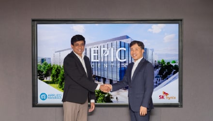
Applied Materials and SK hynix Announce Long-Term R&D Partnership to Accelerate AI Memory Innovation at EPIC Center in Silicon Valley
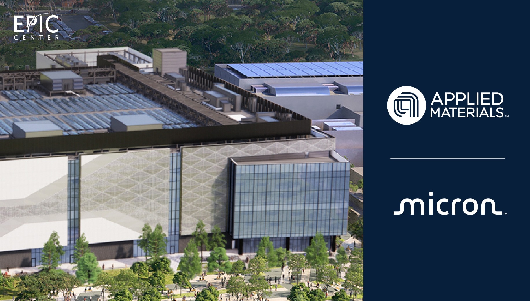
Applied Materials and Micron Partner To Advance U.S. Innovation in Next-Generation AI Memory Solutions
Applied Materials Announces Samsung Electronics Will Join the New, Multibillion-Dollar EPIC Center in Silicon Valley
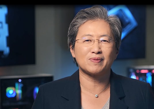
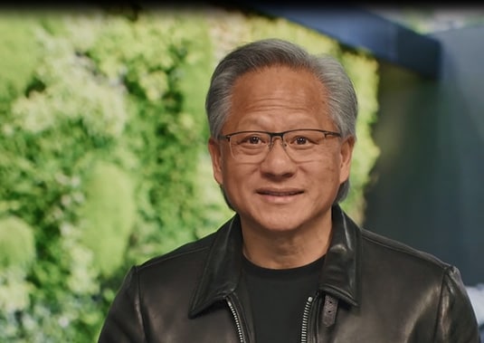
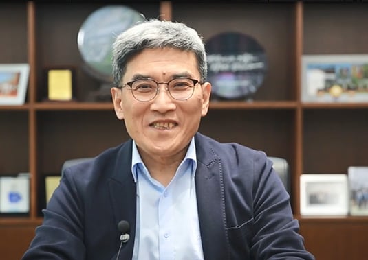
During the May 2023 EPIC Center announcement, leaders from semiconductor and computing companies, along with major universities, shared their thoughts about the importance of this facility and how semiconductor chips are more critical to the global economy than ever before.
Semiconductor and Computing Companies
To watch more leaders share their thoughts, please visit: 2023 EPIC Center Announcement.
Frequently Asked Questions
The Applied Materials EPIC Center—short for Equipment and Process Innovation and Commercialization—is a facility in Silicon Valley designed to accelerate innovation in semiconductor manufacturing. It represents the largest-ever U.S. investment in advanced semiconductor equipment R&D and is designed from the ground up to dramatically reduce the time it takes to commercialize breakthrough technologies from early-stage research to full-scale manufacturing. It does this by increasing speed, accuracy and efficiency through tighter collaboration and faster cycles of learning.
With state of the art cleanroom space for collaborative R&D, the EPIC Center is on track to become operational in 2026. A traditional chip development cycle is a serial compartmentalized process, but the EPIC model and infrastructure will drastically reduce that time, enabling parallel development, agile handoffs and early access to next-generation processes across the ecosystem. This accelerates product roadmaps, increases commercial success rates and amplifies the return on R&D investments.
In the industry, what we work on is constantly changing, but the way we work hasn’t changed much. Applied Materials is changing the rules with the EPIC Center. By enabling earlier access to integrated tools and processes, the Applied Materials EPIC Center helps drive faster innovation cycles and support the industry’s transition to more complex device architectures, like AI.
No. The Applied Materials EPIC Center is focused on research, development, and commercialization, not high-volume manufacturing. It will serve as a bridge between R&D and production fabs.
The Applied Materials EPIC Center has three floors. The top floor is the cleanroom, which has all the tools. The middle level is the subfab with all the equipment that runs those tools. And the lowest floor is like a basement with equipment to run the whole building.