半導體 (Semiconductor)
解決方案與軟體
設計和生產半導體晶片的製造系統
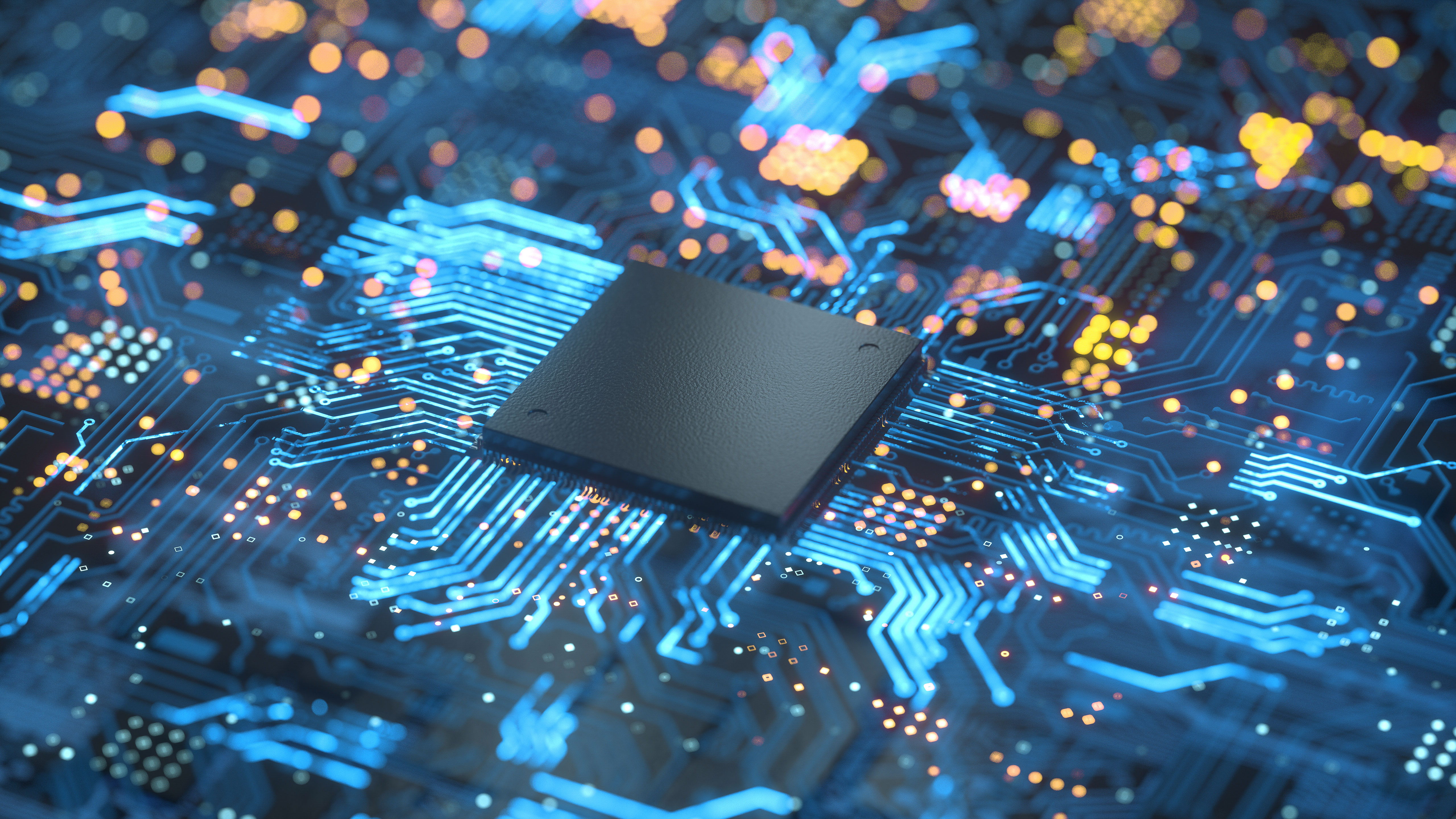
推動 AI 時代
AI 時代需要晶片能源效率與效能迅速且顯著提升。這項挑戰成為應用材料公司以全新方式創新協作,來加速新技術商業化的驅動力。 透過與整個生態系統深度合作,我們將加速推動 AI 時代所需的先進晶片問世。
以技術轉折為重的創新
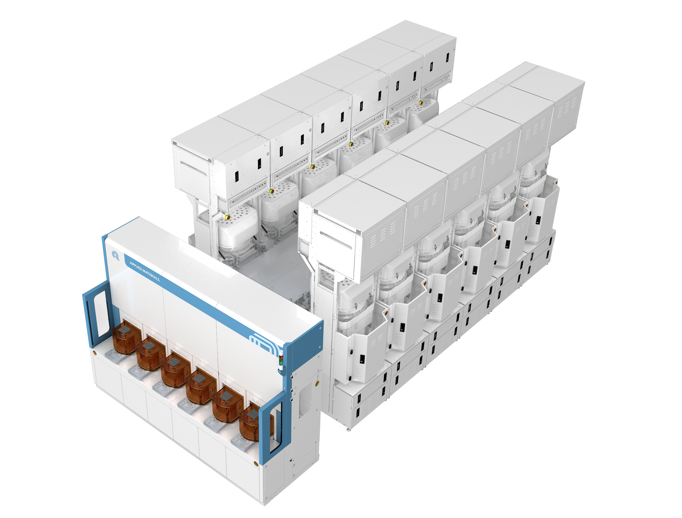
我們透過串連寬廣的能力與技術組合,持續擴展高度差異化解決方案。 我們廣泛且互連的產品組合,能以嶄新方式創建和沉積、成形與移除、改性、分析和連接材料與元件。 憑藉整合於同一平台的製程技術與量測能力,我們的Integrated Materials Solution®(整合材料解決方案)技術能協同優化材料的沉積、移除、改性與分析,創建新材料並打造新結構,以實現高效能、低功耗的先進節點晶片。
淨零加速
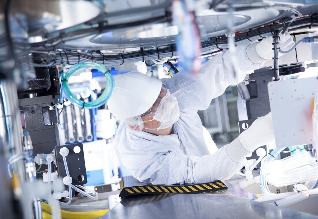
我們的系統設計持久耐用,並可支援升級和重新使用於新的應用。所有新生產的系統元件與零組件都經過精心設計以利維修,我們盡可能使用翻新零件,提升永續性與成本效益。我們持續開發更多適用於晶圓廠和附屬製造區(subfab) 的技術與服務,協助客戶提升其營運永續表現。我們深知,身為業界獨一無二的領導者,肩負對員工、客戶及社會的重大責任。
Unlocking Next-Gen AI Chips Through Advanced Materials Modification
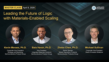
The Angstrom Era Explained: New Master Class Series Kicks Off April 8
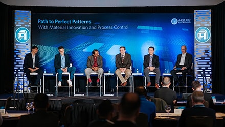
Applied Materials Convenes Industry Leaders on Advanced Patterning for the AI Era