半导体 (Semiconductor)
解决方案与软件
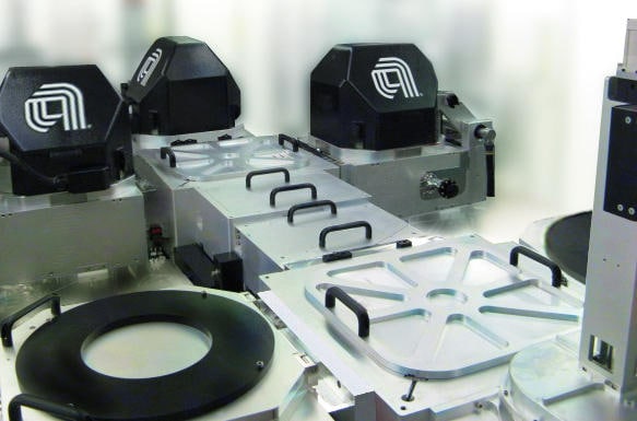
Charger™ UBM PVD
The Applied Materials Charger UBM PVD system defines a new standard in metal deposition productivity and reliability for chip packaging. Specifically designed for UBM, RDL, and CMOS image sensor applications, the Charger system's linear architecture more than doubles the wafer output of competing systems to deliver the highest productivity available. In addition, integration with the latest Volaris™ pre-clean technology allows the system to process more wafers between servicing for best-of-breed uptime and the lowest available per-wafer cost.
The Volaris pre-clean chamber design minimizes contaminants from organic film outgassing and extends best-in-class contact resistance performance from legacy to the most advanced technology nodes compared with traditional inductively coupled plasma sputter chambers. This unique in-situ clean technology extends process kit life, lowers production costs, and increases output by reducing preventive maintenance frequency to give customers the lowest cost of ownership among packaging deposition systems.
Select magnetron and PVD chamber design improvements fulfill exacting film deposition uniformity specifications for various metals used in UBM and RDL applications (e.g., Ti, TiW, Cu, and NiV).
The Charger system's modular architecture enhances configuration flexibility, making it easy to expand a compact three-chamber configuration into a five-chamber, high-volume manufacturing system with minimal downtime.