半导体 (Semiconductor)
解决方案与软件
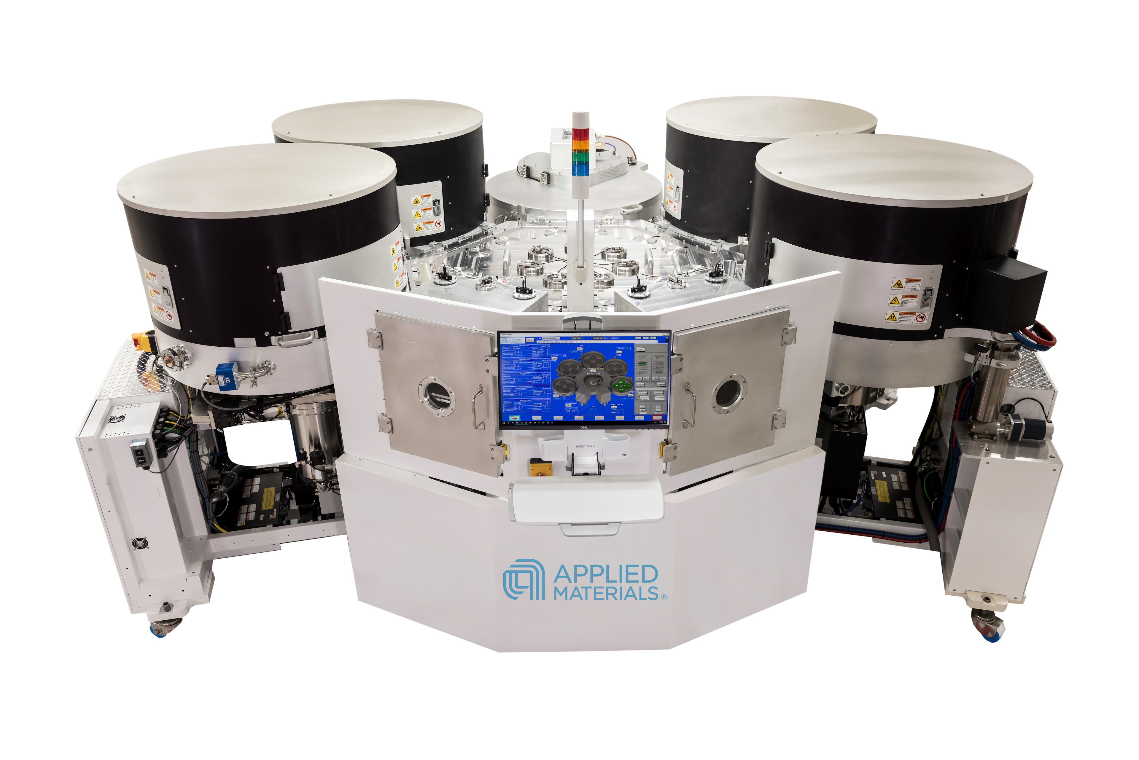
Axcela™ PVD
The best-in-class Applied Axcela PVD system has demonstrated process superiority and stability with non-uniformities of <2% 1σ over the last 10 years. Designed for the lowest cost of ownership and easy serviceability for thick films up to 8µm, each sputter chamber has the standard capability of depositing up to three different materials with the option of co-sputtering for higher deposition rates. The compact system can be configured for 150, 200, 300, or 330mm in many combinations. It includes degas, pre-clean, and PVD chamber modules to accommodate multiple applications, and optimal processing and throughput requirements. This easy configurability allows customers to select the most desirable configuration for a given application.
The Axcela system’s small-batch-cluster architecture makes this highly reliable PVD tool an excellent choice for most metallization applications, including EMI shielding, back side metallization, MEMS, TSV, UBM, and RDL. Deposition thickness can be closely controlled for thin films, enabling process and manufacturing engineers to meet demanding design requirements.
The D-source magnetron promotes high target utilization with full-face erosion. The chamber and target architecture enable maximum collection efficiency of atoms sputtered from the target instead of wasting them on the shields. Magnetron and shield design facilitate the system’s ultra-low particle count.
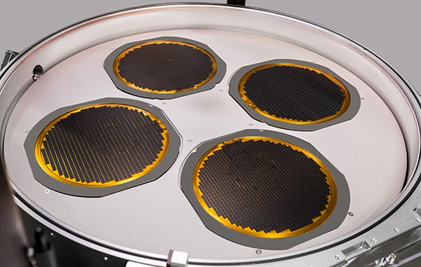
EMI rings with packages in a 200mm and 300mm chamber