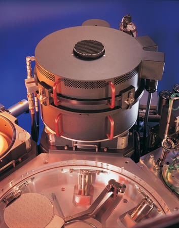
Centura™ Etch
Applied Materials Centura Etch system delivers high-productivity silicon, metal, and dielectric etch. Etching is one of the most critical yet challenging of semiconductor production operations. Whether etching a gate, a transistor isolation trench, a high aspect ratio contact, or any level of interconnect metal or dielectric film, maintaining precise, repeatable, and uniform control of critical dimension is the key to device yield. Designed for 150mm and 200mm wafer sizes, the system addresses technology challenges that include high aspect ratio etch ( <110:1) for a range of MtM applications including all-in-one hard mask open-trench-strip for shallow junction MOSFET, and new materials like indium tin oxide, silicon carbide (SiC), InGaAlP, GaAs, and gallium nitride for power devices and LEDs.
The Centura and Centura AP mainframe single-wafer, multi-chamber architectures enable integrated, sequential wafer processing in up to four process chambers for 150mm, 200mm, and 300mm wafers.
For 150/200mm wafers, Applied Centura DPS DTM system employs advanced deep reactive ion etch (DRIE) for a range of materials to precisely control etch wall smoothness and trench profile, while delivering high aspect ratio capability and achieving high throughput. Applied Centura DPS Plus is the industry standard for metal etch processes.
For 200/300mm wafers, Applied Centura AP mainframe chamber technologies address poly, metal, oxide, and DRIE etch.
These systems feature:
- Enhanced capabilities for handling a variety of substrates, including III-V materials, reliably and carefully from load lock wafer mapping to clear wafer orientation to wafer placement
- Booster kit with columbic-type ceramic ESC and yttrium-coated process chamber
- EyeD™ advanced full-spectrum endpoint and PC Toolset for chamber-state analysis
- Turbomolecular pump for enhanced temperature control of byproducts with blade design to reduce back streaming
- ESC with larger wafer contact area and dual gas feed for better within-wafer performance control
- Top RF source for higher etch rates and in-situ cleans

