Products & Technologies
Products & Services
Contact
Products & Services
Products & Technologies
Services
Resources
Contact
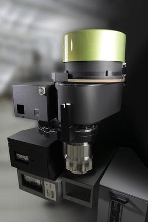
Centura® Silvia® Etch
TSV offers product designers a new and highly space-efficient degree of freedom by enabling integration of circuit components from various nodes, boosting functionality and performance beyond those obtainable from wire bonding and flip chip 3D schemes.
In the drive to maximize the functionality-to-volume ratio, device makers are integrating chips using multiple schemes. TSV technology enables 3D interconnects by creating vertical pathways functioning as components of the integrated circuit to connect stacked chips or wafers.
The Applied Centura Silvia Etch system is specifically designed for the challenging deep silicon etch required to create the vertical connections between the chips or wafers. It overcomes the tradeoff between profile control and high etch rate faced by conventional methods. The system’s high-density plasma source enables the highest silicon and oxide etch rates for all wafer-level packaging applications.
Silvia leverages Applied’s long-standing experience as a leading-edge innovator and market leader in deep silicon etch and TSV production expertise to optimize the etch performance needed for 3D interconnect etch applications. With etch processes accounting for approximately 15% of the TSV manufacturing sequence, the substantial reduction in cost of ownership derived from Silvia’s throughput and consumables-free process kit makes a major contribution to lowering customers’ overall cost of implementing TSV technology.