Products & Technologies
Products & Services
Contact
Products & Services
Products & Technologies
Services
Resources
Contact
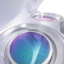
Producer® Eterna® FCVD™
With the Eterna FCVD system, Applied continues its decade-long leadership in delivering gap-fill technology advances to the semiconductor industry. These innovations have provided customers with unique, simplified, and cost effective solutions to meet the challenges of multiple chip generations.
Chip manufacturers are continuously designing chips with smaller and smaller transistors to gain more functionality per square millimeter. As the transistors shrink, so do the spaces between them, making it increasingly difficult to physically isolate them from one another. Filling the tiny and often irregularly shaped spaces (gaps) between transistors with a high‑quality dielectric is becoming increasingly challenging and a new solution is required for chip designs for 20nm and below.
The Applied Producer Eterna Flowable CVD system answers this challenge with the only technology that ensures complete, void-free fill of these critical gaps. The unique Eterna FCVD process fills gaps with extreme dimensions, having aspect ratios of up to 30:1, including those with highly irregular or complex profiles.
The new process deposits a high-quality dielectric film in a liquid-like state on the wafer surface, allowing the film to readily flow into the gap, filling it completely without voids or seams. The careful choice of chemistry used creates an extremely pure, robust, carbon-free, dielectric film to ensure reliable electrical isolation and compatibility with subsequent process steps (e.g., CMP).
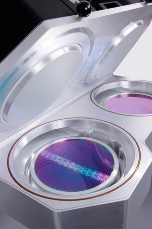
The Eterna FCVD process is available on Applied’s benchmark Producer GT platform, which is highly regarded in the industry for its exceptional productivity.
- 1 / 2
- 2 / 2