Products & Technologies
Products & Services
Contact
Products & Services
Products & Technologies
Services
Resources
Contact
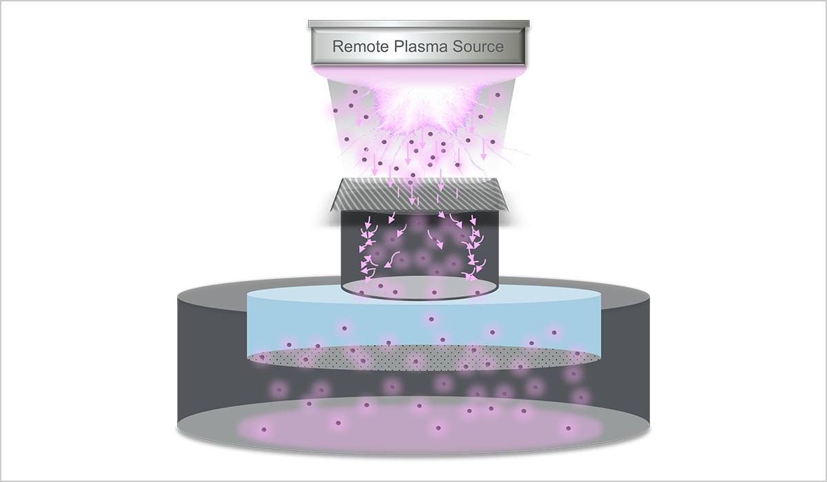
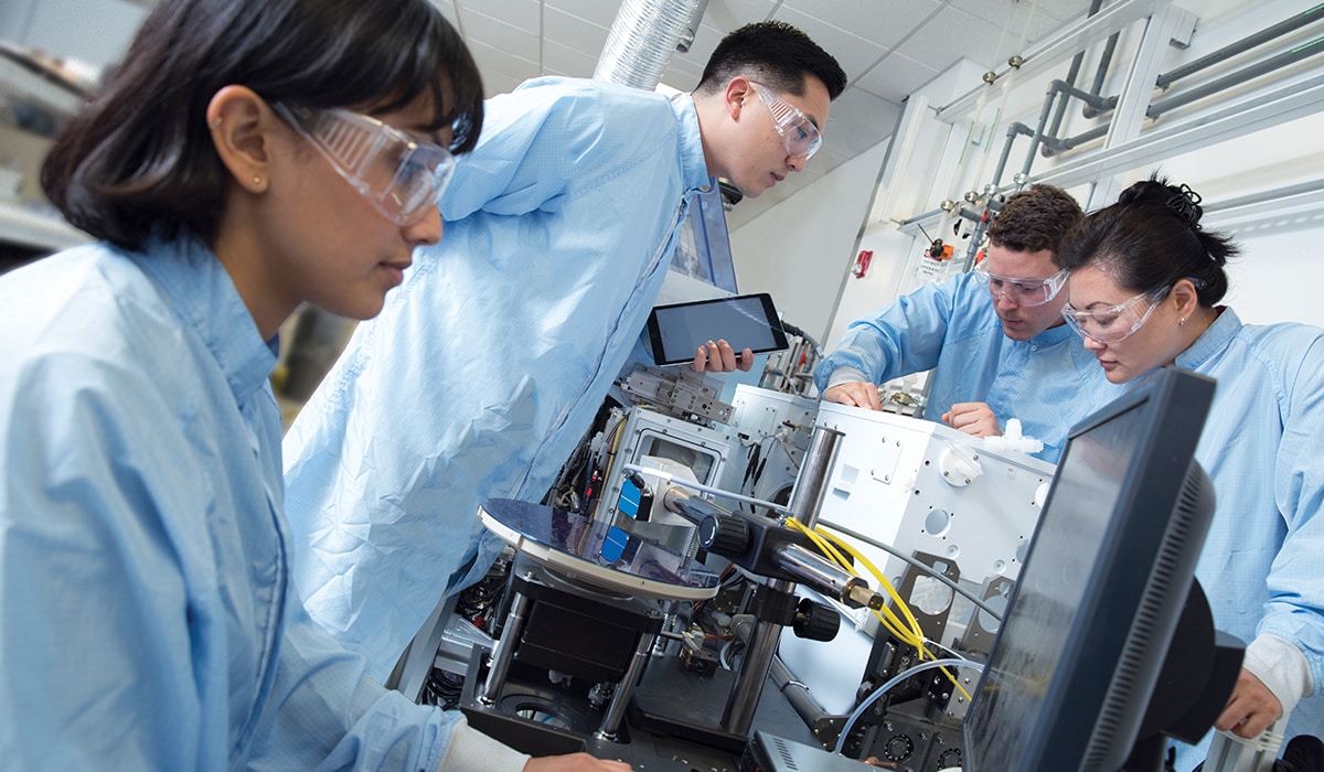
Unlocking Next-Gen AI Chips Through Advanced Materials Modification
Andy Lo • April 2, 2026
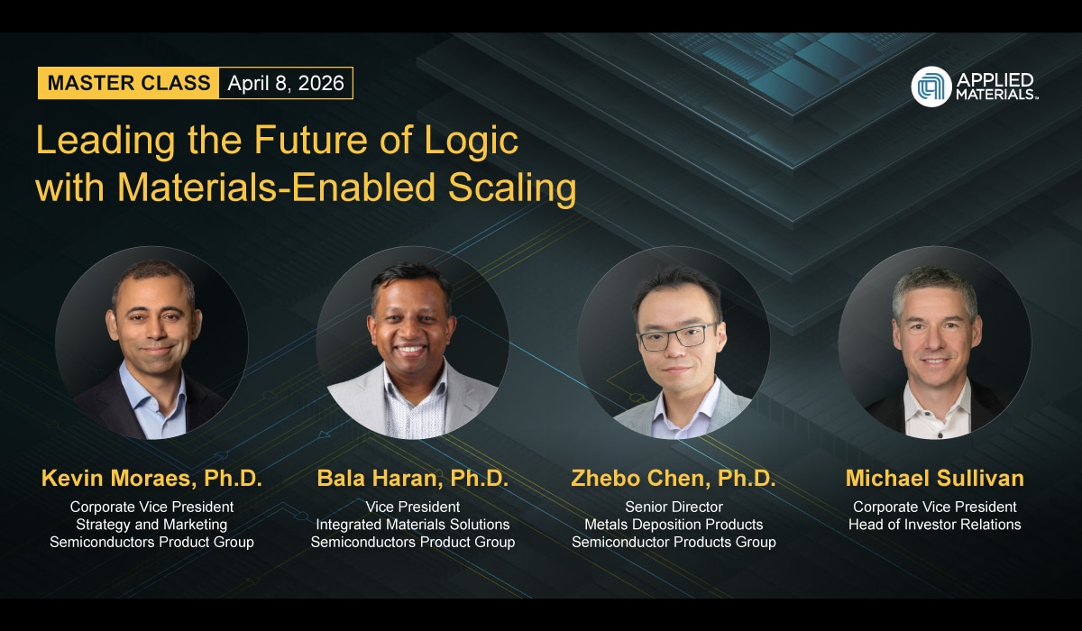
The Angstrom Era Explained: New Master Class Series Kicks Off April 8
Newsroom Staff • March 30, 2026
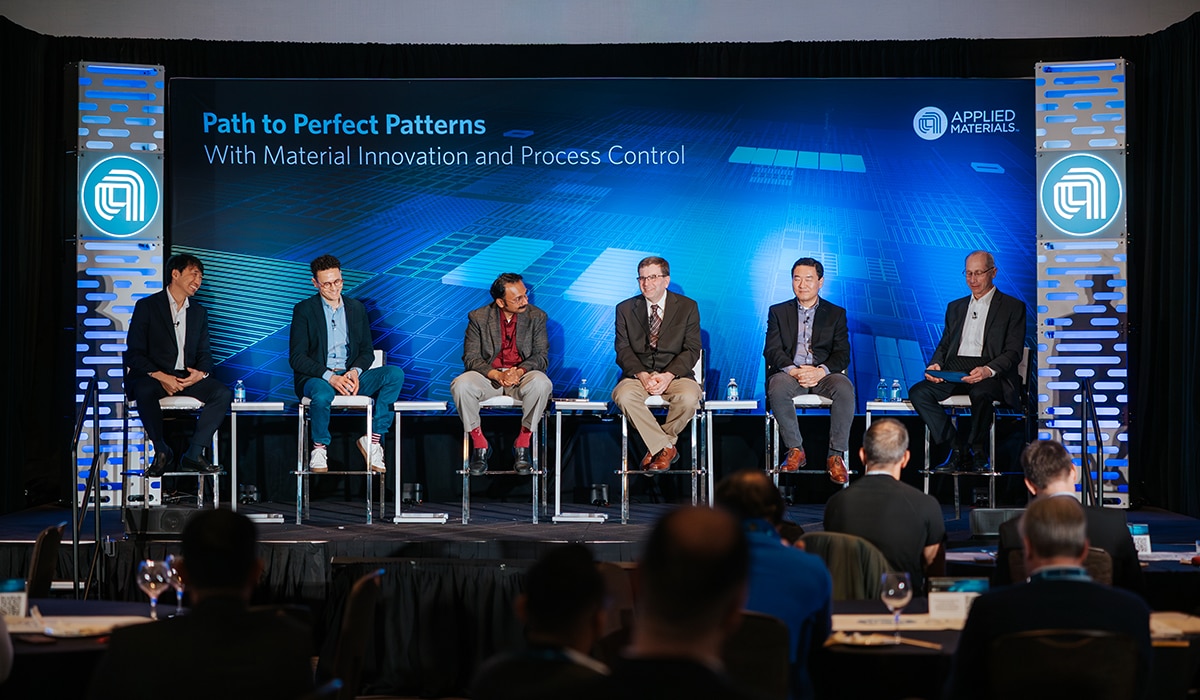
Applied Materials Convenes Industry Leaders on Advanced Patterning for the AI Era
Newsroom Staff • March 24, 2026
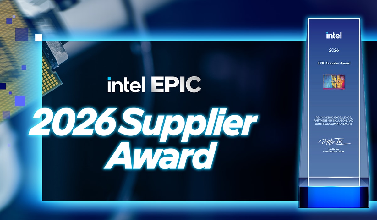
Applied Materials Receives Intel EPIC Supplier Award
Applied Materials Accelerates Materials Simulation for the AI Era in Collaboration with NVIDIA
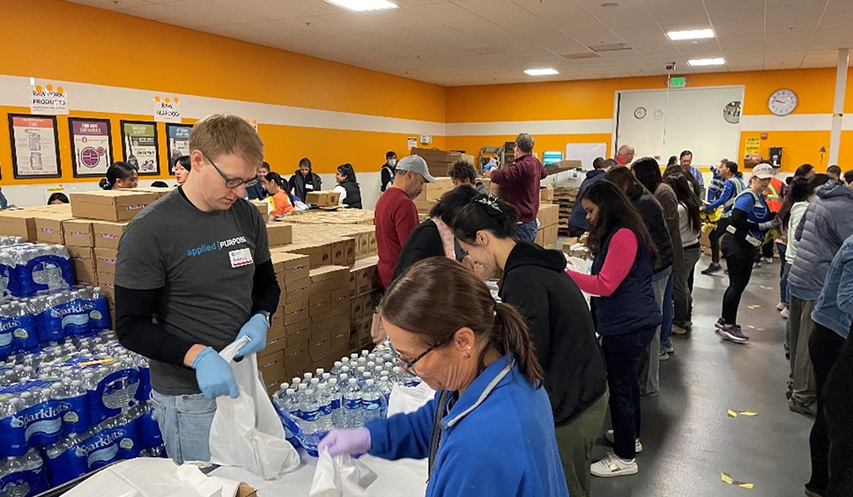
Going “All In”: How Applied Materials is Turning Hunger into Hope

Precision from the Bottom Up: Enabling Angstrom-Era AI with Sym3™ Z Magnum™

Powering the Next Era of Contact Scaling with ALD Molybdenum
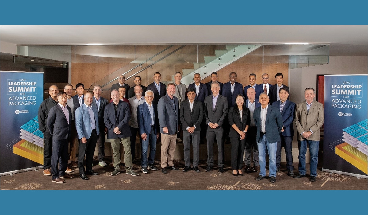
Future of Advanced Packaging: Industry Insights on Co-Innovation and Talent Development
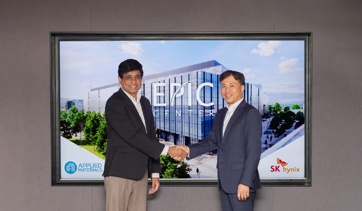
Applied Materials and SK hynix Announce Long-Term R&D Partnership to Accelerate AI Memory Innovation at EPIC Center in Silicon Valley
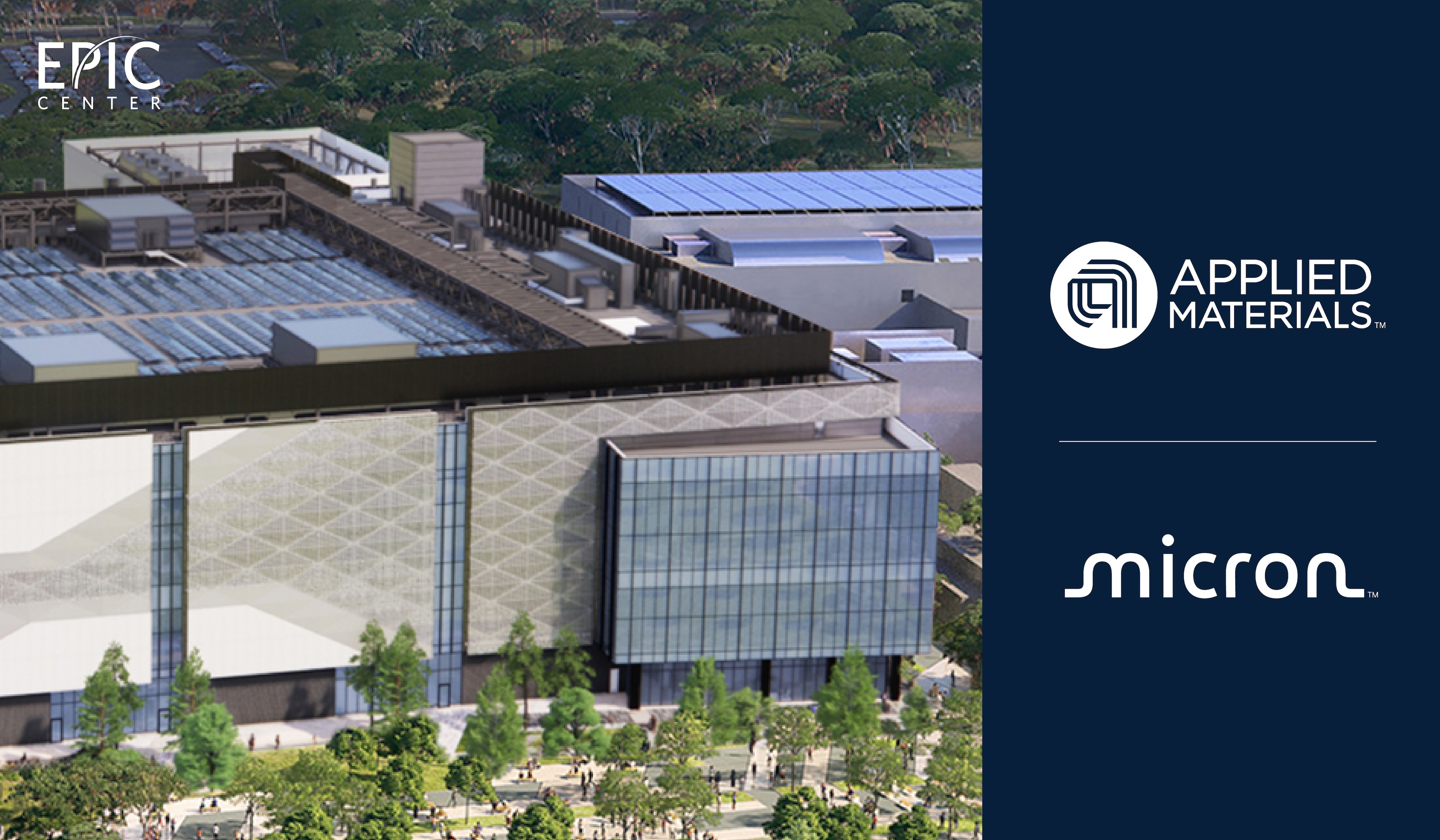
Applied Materials and Micron Partner To Advance U.S. Innovation in Next-Generation AI Memory Solutions

Applied Materials Raises Quarterly Cash Dividend by 15 Percent

Contact Media Relations
Media and analyst inquiries, including requests for images and b-roll, can be directed to Media_Relations@amat.com