Products & Technologies
Products & Services
Contact
Products & Services
Products & Technologies
Services
Resources
Contact
Posted
September 12, 2019

Stay updated on our content.
Themes of an AI Summer: VC Perspectives

Sep 12, 2019
It’s been a busy summer for Applied Ventures. Our team has had many interactions in the startup and investing space, and added some new companies to our portfolio. I’ll be sharing highlights of these activities in a series of upcoming blogs, but first I’d like to reflect on current market developments in machine learning and how they are affecting VC investment patterns.
Strategic Investments in Semiconductor Startups Continue
In my last blog post about VC opportunities in the AI developer ecosystem, I explored why VC funding, particularly from corporate and strategic investors, is flowing into AI hardware companies, and how different kinds of VCs approach the space. The pace of strategic investment from Corporate Venture Capital (CVC) into AI companies has not slowed down, with 2018 ending well above 2017 levels. According to data published by CB Insights, CVCs deployed $5.1B across 291 AI-related deals in 2018.
Although the data point above does not differentiate between investment levels in software and hardware companies, a rough count of the top five hardware startups puts the total for 2018 over $500M. More recent financings indicate that chip investing remains a priority for CVCs.
My colleagues Buvna Ayyagari-Sangamalli, Sundeep Bajikar, Sanjay Natarajan and David Thompson have all noted in previous blogs that the inflection of AI brings new requirements that have enabled a flourishing of variant approaches to computer architecture and design. Startups continue to explore market verticals and innovate their hardware, and for now they are mainly doing so in system-level architecture, while leveraging process technologies at foundries that are available, mature and cost effective. Data gathered in a survey by KPMG found AI chip companies taping out products at a variety of process nodes, some of them employing more than one level of process technology for their chips. While trailing-edge process technology (>14nm) continues to be sufficient for demonstrating the potential of radically specialized system-level architectures, some startups such as Esperanto Technologies have announced plans to move directly to 7nm for their first product runs to get ahead of the competition.
As startups and large companies introduce custom chip products for the datacenter as well as edge applications, we continue to see almost all of the resources and capital aimed at machine learning inference rather than training. Why would this be? Part of the reason is a significant head start in developer frameworks that helps to keep training workloads on GPUs. Another factor is the opportunity for differentiation, i.e. the target market a startup hopes to “own.” There are relatively few commonly used training frameworks, while the number of plausibly useful inference models created by those networks is essentially endless. To paraphrase Google Engineer Pete Warden, if the growth of training is proportional to the number of ML developers, inference grows proportionally to the number of ML users. That doesn’t mean that disruptive approaches to address training inefficiency aren’t of interest to VCs, as indicated by some well-funded startups like Habana Labs and the recently out-of-stealth Cerebras, which announced its 15kW, 1.2 trillion transistor wafer-scale processor at this year’s Hot Chips conference. Nevertheless, most investors that I’ve spoken to believe that the potential market size and reach for inference is currently much greater.
Some of these observations are borne out in a report by McKinsey published in December 2018. In the report, McKinsey estimates that the present market size for datacenter inference is 4-5x larger than training, although over the next half decade, datacenter training TAM may grow twice as fast on a revenue basis. The report also estimates that the nascent edge inference market could grow from essentially nothing today to over a $4B TAM by 2025. In just six years from now, that would be comparable to what the datacenter inference chip market is like today. Edge training, which may include software approaches such as federated learning, could also spur development of new ASICs that offset the demand for datacenter training chips.
Emergence of Edge AI Products: Energy Efficiency and Managing the Flow of Data Are Key
Recent venture funding of edge compute focused startups are a strong signal for the emergence of intelligent edge as a distinct market vertical. Why would it be a new category and how could its component technology diverge from traditional semiconductor products like CPUs, MCUs or mobile application processors?
The definition of “edge compute” has traditionally meant the very end of the outer fringe of the hard-wired network, such as a PC on a desk at home. However, the edge use case of today has seen the growth of more powerful compute in tiny, ultra-mobile and remote applications. Markets for these products force designers to make tradeoffs between network connectivity, physical size and power consumption, either because of the product form factor or operating conditions. Regardless of whether or not a device has easy access to the internet, at a minimum data will be captured at the edge and the cost of streaming so much compressed data (just one HD smart cam can generate tens of GBs per day) to the cloud often becomes prohibitive. It then becomes advantageous to enable data structuring (such as classifying and labeling images) at the point of capture. While some edge applications like remote sensors may be relatively more power constrained than others and can sacrifice absolute accuracy to save battery life, others like vehicle guidance may have to put responsiveness (low latency and small batch size) above everything else.
Although trying to define rigorously what is “edge” often provides more exceptions than adherents to the rule, it generally refers to chips that balance power consumption and memory use at the expense of absolute computational throughput. Memory inefficiencies are almost universally seen as a key area of opportunity by AI/ML practitioners, as the matrix calculations that are a mainstay of inference algorithms require rapidly swapping large images or other datasets in and out of memory. From startups to end users, there is a general trend towards making low-latency memory more accessible by relocating it closer to the compute circuitry and adopting technologies for densifying those banks of RAM. In a January 2019 Forrester study commissioned by Micron, 89 percent of respondents to a survey of IT experts ranked memory proximity to compute as “Important” or “Critical” in processing AI/ML workloads. The belief was more acute among respondents who were currently running advanced analytics at the edge, where the belief rose to 95 percent of respondents.
In my next blog, I will discuss some of Applied Ventures’ recent interactions with startups and the VC community related to AI hardware.
Tags: Applied Ventures, vc, artificial intelligence, AI hardware

Michael Stewart
Now is the Time for Flat Optics
For many centuries, optical technologies have utilized the same principles and components to bend and manipulate light. Now, another strategy to control light—metasurface optics or flat optics—is moving out of academic labs and heading toward commercial viability.
Seeing a Bright Future for Flat Optics
We are at the beginning of a new technological era for the field of optics. To accelerate the commercialization of Flat Optics, a larger collaborative effort is needed to scale the technology and deliver its full benefits to a wide range of applications.
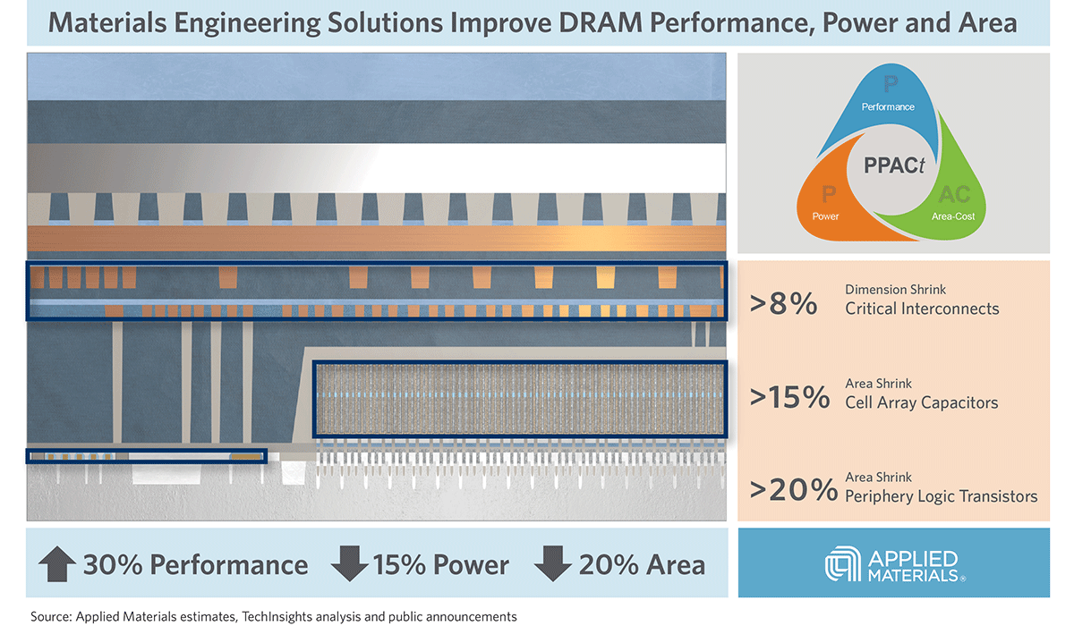
Introducing Breakthroughs in Materials Engineering for DRAM Scaling
To help the industry meet global demand for more affordable, high-performance memory, Applied Materials today introduced solutions that support three levers of DRAM scaling.