Products & Technologies
Products & Technologies
Services
Resources
Posted
August 21, 2019

Stay updated on our content.
The AI Paradox

Aug 21, 2019
Are we ready for the biggest opportunity of our lifetime?
That’s the question Applied Materials CEO Gary Dickerson asked at the beginning of his keynote speech at this year’s AI Design Forum™, in San Francisco. Gary’s been traveling the world talking to chipmakers and policymakers about a $10 trillion question: how do we capture the economic opportunity of AI, which will transform nearly every industry and institution over the coming years?
The opportunity comes with formidable challenges that Gary called the “AI Paradox”; we won’t realize the benefits of AI unless we address the challenges.
One challenge involves the energy this new era will demand—from the billions of new edge devices sending zettabytes of data to the cloud for processing—and the data centers that will train machine learning algorithms and run inferencing workloads. Gary presented a scenario based on this data growth and no further breakthroughs in energy efficiency, illustrating how AI data centers could consume more than 10 percent of global electricity supply by the year 2025. This potential 500 percent increase from today’s levels puts new pressure on the computing industry to deliver major improvements in system performance-per-watt at a time when classic Moore’s Law scaling is running out of gas. To do its part, the chip industry needs a new playbook for semiconductor design and manufacturing—one that involves a combination of techniques—to improve semiconductor performance, power and cost.
A second challenge Gary put forth is the need to accelerate the pace of innovation by a factor of 10, not just in chip design and manufacturing, but throughout the entire computing industry value chain—from materials to systems. This need for innovation and cooperation throughout the ecosystem is the rallying concept of the AI Design Forum and was echoed throughout the day by speakers ranging from chipmakers to design software leaders, IP companies and cloud service providers. The companies that step out of their traditional silos to connect better and faster will be the winners in the AI Era.
Accelerating innovation also means shortening the time it takes to bring new computing technologies from lab to high-volume fab. As Gary pointed out, there is a tremendous difference between creating a new chip structure or 3D device in a lab and publishing a paper—and building billions of reliable devices at high yield. Applied is helping solve these challenges for emerging memories like MRAM, PCRAM and ReRAM with Integrated Materials Solutions: systems that combine a variety of process chambers in high vacuum to deposit and modify new materials to enable these new types of chips, which in turn reduce the power needs of edge devices and cloud data centers.
One thing is certain: the industry can’t address the AI Paradox by looking to the past. We have to think differently and connect differently than we ever have before in order to enable the future. Stay tuned for more blogs that dive deeper into the concepts Gary put forth at this year’s AI Design Forum. In the meantime, you can watch a video of his keynote below.
Tags: AI Design Forum, AI Era, New Playbook, MRAM, PCRAM, ReRAM
Applied Materials
Corporate Communications

The Applied Materials team publishes posts of general interest to our readers.

Now is the Time for Flat Optics
For many centuries, optical technologies have utilized the same principles and components to bend and manipulate light. Now, another strategy to control light—metasurface optics or flat optics—is moving out of academic labs and heading toward commercial viability.

Seeing a Bright Future for Flat Optics
We are at the beginning of a new technological era for the field of optics. To accelerate the commercialization of Flat Optics, a larger collaborative effort is needed to scale the technology and deliver its full benefits to a wide range of applications.

Introducing Breakthroughs in Materials Engineering for DRAM Scaling
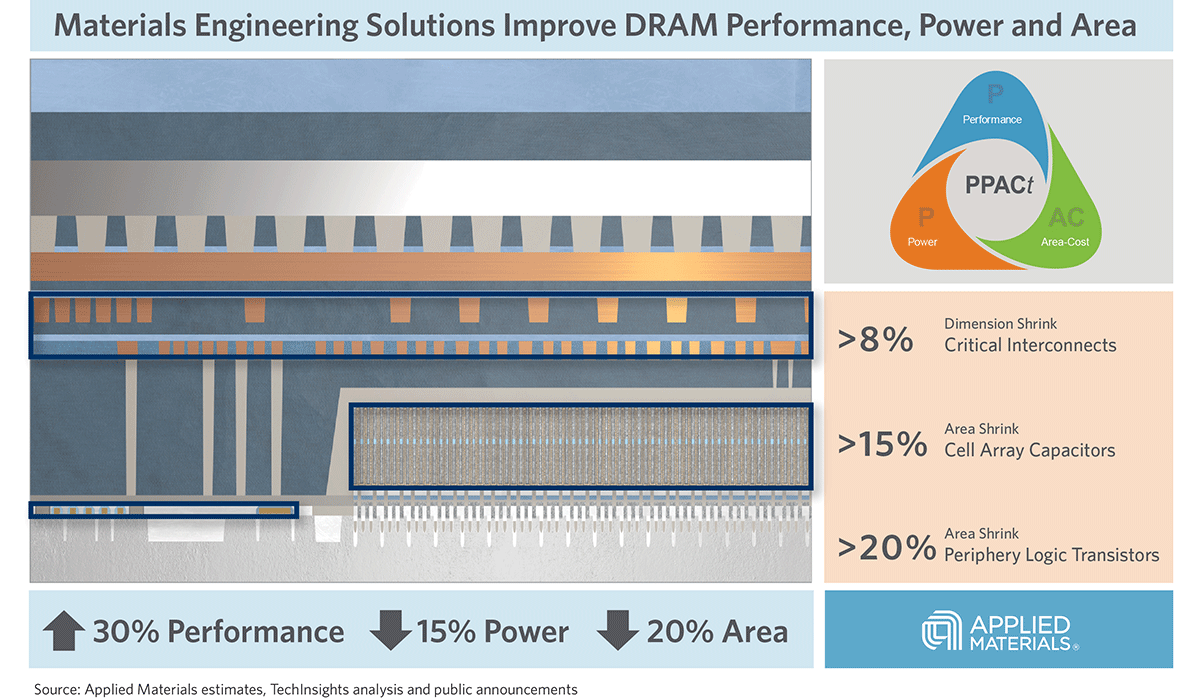
To help the industry meet global demand for more affordable, high-performance memory, Applied Materials today introduced solutions that support three levers of DRAM scaling.
