Products & Technologies
Products & Services
Contact
Products & Services
Products & Technologies
Services
Resources
Contact
Posted
April 19, 2022

Stay updated on our content.
Newer Ways to Shrink
Apr 19, 2022
In a blog previewing our upcoming “New Ways to Shrink” Master Class, my colleague Regina Freed explained that classic 2D Moore’s Law scaling with EUV can continue well into the future—as long as we also address 6 key issues in materials engineering and metrology.
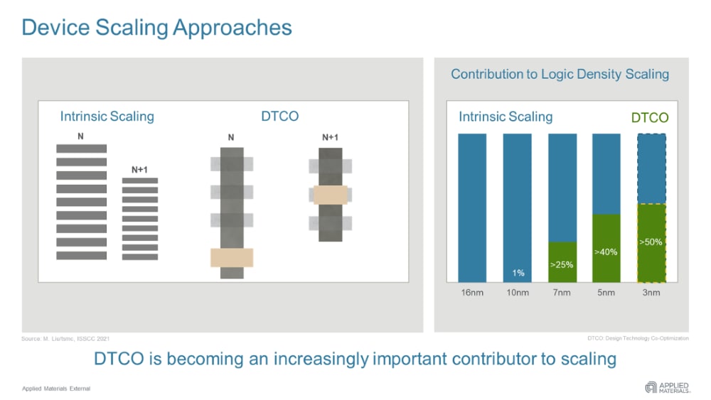
At the 3nm node, 50% of logic density improvements are from “intrinsic scaling”—which is classic 2D scaling—and 50% are from “DTCO”—or design technology cooptimization. While intrinsic scaling has served the industry well for more than 50 years, DTCO is a more recent phenomenon that is helping compensate for the slowing of classic Moore’s Law. DTCO gives us newer ways to shrink logic cells, increase density and improve area-cost.
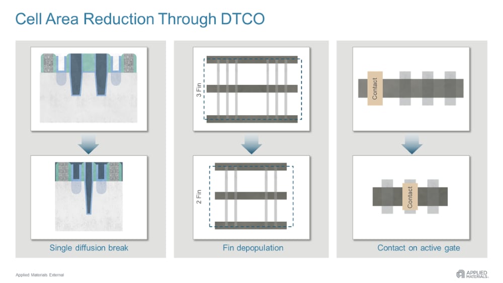
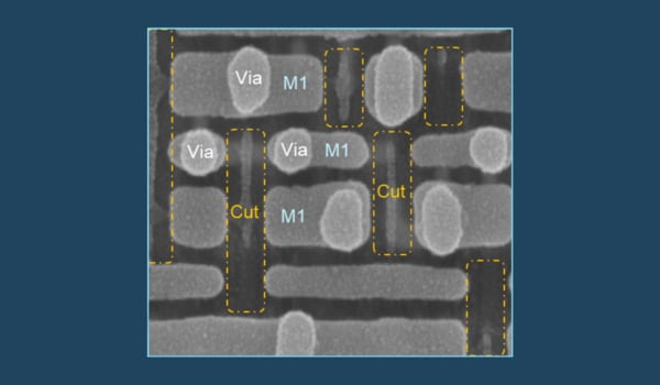
DTCO involves clever changes in the layout of logic cell elements to enable further transistor scaling independent of lithographic pitch. Several DTCO techniques can already be found in chips today. For example, in isolating individual logic cells, designers have replaced double diffusion breaks with single diffusion breaks—providing obvious scaling benefits. Designers have also implemented fin depopulation, reducing the number of fins per transistor from three to two. Likewise, designers have pursued contact over gate, moving the transistor’s electrical contact from the side to the top.
In my portion of the April 21 Master Class, I’ll discuss two emerging innovations that use DTCO concepts to increase logic density—while also improving chip performance and power consumption.
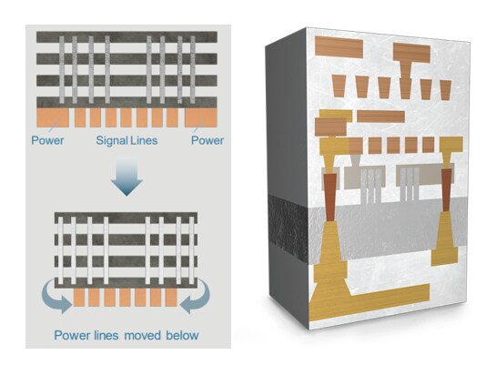
Backside Power Distribution Networks
Transistors and logic cells sit at the bottom of the wafer. Today, power and signals are both routed from above, cascading through each metal layer of a chip. The thicker power lines provide the current needed to switch, while the thinner signal lines determine when to switch.
At each metal layer there is electrical resistance, and some of the supply voltage is lost. This wastes power and creates heat. In backside power distribution networks, the thicker power lines are re-routed, using the back side of the wafer to reach the transistors from underneath. The industry expects this DTCO wiring innovation to reduce power consumption by as much as 25% while simultaneously increasing logic density by 6-30%, depending on the approach. In our May 26* Master Class, my colleague Dr. Mehul Naik will explain how backside power distribution networks are engineered.
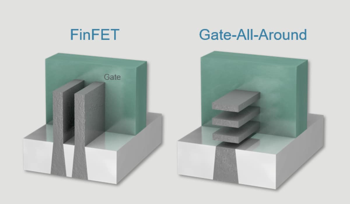
Gate-All-Around Transistors
Gate-All-Around (GAA) transistors will be one of the chip industry’s biggest design inflections since the introduction of FinFETs in 2010, which signaled the shift from planar 2D transistors to 3D transistors.
It may seem counterintuitive to describe GAA as a form of DTCO, but it meets the definition because GAA cleverly rearranges the elements of the transistor in a way that increases logic density versus FinFET at an equivalent lithographic pitch. Fortunately, it also comes with materials engineering innovations that greatly improve power and performance. In this blog, I’ll describe the area savings, discuss the greater use of epitaxy and selective materials removal, and explain how Integrated Materials Solutions help GAA transistors do more in less space.
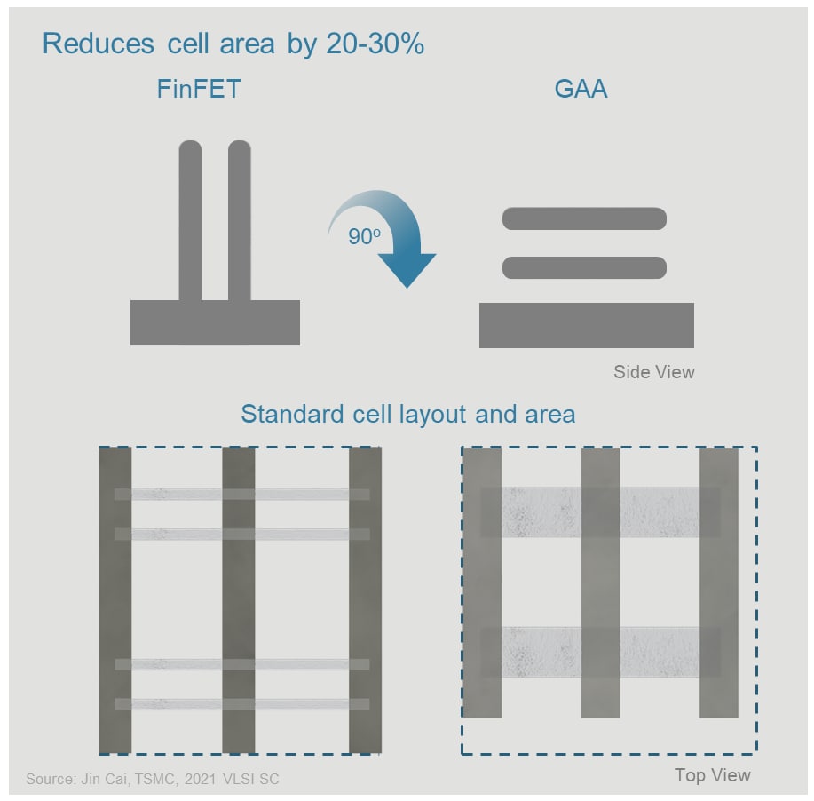
Conceptually, GAA is like rotating a FinFET transistor by 90 degrees. The gate surrounds the silicon channels on all four sides—which is an improvement over FinFET which can only surround three. The DTCO benefit is that the logic cells shrink in both the X and Y dimensions. Designers can aggressively reduce area-cost while keeping performance the same. Or more likely, they may widen the nanosheets to increase drive current, thereby increasing performance by as much as 25% while increasing density by around 25% as well.
Epitaxy and Selective Removal are Critical to GAA Power and Performance
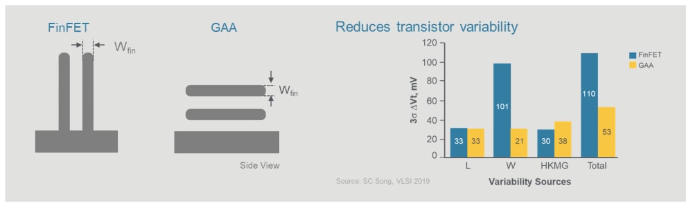
From a manufacturing perspective, GAA borrows many of the proven processes used to make FinFETs. However, a key difference is how the width and uniformity of the silicon channels are determined and controlled. With FinFETs, the channel width is determined by lithography and etch; there tends to be variability which reduces transistor performance. With GAA, the channel width is defined by epitaxy and selective removal which are more precise, enabling higher channel uniformity and transistor performance.
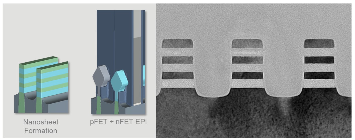
GAA employs two kinds of epitaxy. Fast, blanket epitaxy is used to deposit alternating layers of silicon and silicon germanium to form nanosheets. Later, slow, selective epitaxy is used to apply strain engineering to the nanosheets to help optimize transistor performance. Eventually, selective materials removal is used to remove the silicon germanium layers which are sacrificial—used only to help form and shape the silicon channels that electrons flow through when the transistor is in its on state.
Integrated Materials Solutions: New Ways to Shrink the Gate Oxide and High-k Metal Gate
The channels need to be further engineered to complete the transistor. We need to deposit a gate oxide layer to surround the channel on all sides. The thinner the gate oxide, the higher the drive current—which optimizes switching performance—and the lower the leakage current—which affects power consumption and heat. In fact, gate oxide scaling has been stalled for years, and a breakthrough would be good news for chipmakers.
Then the gate oxide needs to be surrounded by a high-K metal gate stack which controls the on-off state of the transistor. Engineering the gate is extremely difficult because the space between the GAA channels is typically just 10nm—much smaller than with FinFETs. The width of the metal gate stack needs to be engineered to optimize chip power and performance for specific end markets ranging from battery-powered mobile devices to high-performance servers. The industry needs a solution to enable threshold tuning in the impossibly small spaces required.
How Much Further Can we Shrink Transistors and Chips?
In summary, our April 21 Master Class will detail two ways to shrink: by pushing classic 2D Moore’s Law scaling with EUV, and by employing DTCO techniques to increase logic density independent of lithographic pitch—as with backside power distribution networks, GAA transistors, and future transistor concepts such as forksheet and CFET. Now that EUV is here, patterning is not the limit. Instead, we are challenged by exponential increases in resistance that accompany ever-smaller transistor contacts and wiring. These challenges will be addressed our May 26* Master Class—along with backside power distribution networks and heterogeneous integration.
* Projected date
Tags: DTCO, gate-all-around, GAA, FinFET, Backside power, materials engineering, Epi, selective removal, Logic scaling
Uday Mitra, Ph.D.
Vice President, Engineering

Dr. Mitra is a Vice President of Engineering at Applied Materials. He has nearly 4 decades of experience in the semiconductor industry managing technology integration, lithography, etch, thin films and packaging modules for both logic and memory products. Prior to joining Applied in 2005, he was director of technology integration at Intel Corporation, where he spent 17 years holding various management positions. Uday received his Ph.D. in materials science from MIT and is a recipient of the Henry Marion Howe Medal from the American Society of Materials International.

Adding Sustainability to the Definition of Fab Performance
To enable a more sustainable semiconductor industry, new fabs must be designed to maximize output while reducing energy consumption and emissions. In this blog post, I examine Applied Materials’ efforts to drive fab sustainability through the process equipment we develop for chipmakers. It all starts with an evolution in the mindset of how these systems are designed.
Innovations in eBeam Metrology Enable a New Playbook for Patterning Control
The patterning challenges of today’s most advanced logic and memory chips can be solved with a new playbook that takes the industry from optical target-based approximation to actual, on-device measurements; limited statistical sampling to massive, across-wafer sampling; and single-layer patterning control to integrative multi-layer control. Applied’s new PROVision® 3E system is designed to enable this new playbook.
Breakthrough in Metrology Needed for Patterning Advanced Logic and Memory Chips
As the semiconductor industry increasingly moves from simple 2D chip designs to complex 3D designs based on multipatterning and EUV, patterning control has reached an inflection point. The optical overlay tools and techniques the semiconductor industry traditionally used to reduce errors are simply not precise enough for today’s leading-edge logic and memory chips.