Products & Technologies
Products & Services
Contact
Products & Services
Products & Technologies
Services
Resources
Contact
Posted
December 18, 2018

Stay updated on our content.
Looking Ahead to the Next 25 Years in Electronics

December 18, 2018
Each year, the IEEE International Electron Devices Meeting (IEDM) holds panel discussions to explore the future of technology. This year, I was honored to be the moderator of a panel featuring some of the best minds in the industry predicting what may exist in 25 to 35 years.
Each of the panelists looked ahead while also remembering the state of electronics two or three decades earlier in their careers, and how developments took unexpected turns. In this blog I’ll focus more on the forward-looking perspectives.
Looking to the future, one topic several panelists commented on was a second revolution coming in electronic design automation (EDA). The last one happened about 30 years ago. Fast forward to now and some believe EDA will be more highly automated and widely accessible, allowing students, for example, to quickly design monolithic integrations of logic and memory targeted to a manufacturable process. High-level descriptions of design could go to layout with no human intervention at all. In some cases, these chips could be incorporated into systems created collaboratively, in an open source environment, and made with 3D printers. Software will configure itself.
This renaissance in hardware will need a new design approach so engineers can develop sophisticated chips that don't take a thousand engineering-years. As communications improve, these new designs can be completed by teams located all around the world and a kind of egalitarianism will take hold, allowing skilled engineers to learn, live and work virtually anywhere.
Energy Harvesting Will Be Sufficient
Another topic discussed was figuring out ways to power things around us all the time. Imagine power embedded within environments so people can charge their devices constantly wherever they are. In 25 years, intelligent glasses and other forms of systems, many of them hands-free devices, could replace smartphones. Such systems will be 10,000 times more energy efficient than what we can achieve today. Because of this energy efficiency, systems will be able to harvest enough energy from the environment to function.
To get to this point, we need dramatic energy efficiency improvements in performance per watt. At Applied Materials, this gap is something we are focused on helping to close using our expertise in materials engineering.
Thinking on Multiple Vectors
Several panelists noted that while the last few decades in the electronics industry have been fun, they have also been difficult, revolving around challenges of Moore’s Law scaling. And, they acknowledged the challenges are becoming much more diverse.
Technologists thus far have been conditioned to think the only way to improve is to shrink, shrink, shrink. Going forward we have to think of improvements on multiple vectors. This is because the rising demand of AI and Big Data are so great.
Several panelists mentioned an emerging contributor to the Big Data challenge: the increasingly important intersection between electronics and health, with faster and less-costly DNA sequencing providing benefits well beyond what is possible with current genomics. Sensors will be everywhere, including the likelihood that implanted chips and environmental sensors will provide a boon to human health.
Within 10 years, compute as we know it today cannot sustain the growth of Big Data and a revolutionary approach of bringing compute into memory makes a lot of sense. But this will be a lot harder than we think. The industry needs a large population of young engineers who can think from scratch to develop these new systems.
One thing is for sure: the people who entered their careers 25 or 30 years ago were born into one world and will leave from another world. As I said when I opened the IEDM panel, we have lived through a unique period in human history, a time unlike anything seen in the last 10,000 years. Now, we just need to work together as an industry in new ways to accelerate the pace of innovation.
The good news is from real-time polling of the audience asking the same question as last year: “Would you encourage your children to take up careers in the semiconductor industry?” 53 percent said yes, compared to 30 percent in 2017—a clear sign that more people are enjoying their work and find careers in electronics rewarding.
Tags: Semiconductors, Big Data, Moore’s Law, electronic design
Sanjay Natarajan
Corporate Vice President, Transistor, Interconnect and Memory Solutions

Sanjay Natarajan is a corporate vice president at Applied Materials, with responsibility for transistor, interconnect and memory solutions. He and his team are driving deeper collaborations with customers and developing new innovations that help enable ongoing improvements in semiconductor devices. Sanjay has published numerous papers in science and engineering journals and holds several patents in the area of advanced high-performance semiconductor fabrication technology. He plays an active role in Science, Technology, Engineering and Math (STEM) education with the local academic community, and is a Research Professor at Portland State University, conducting research in the exciting new field of 3D Bioprinting, using 3D printers to print viable human tissues and organs. He is an IEEE member and has served on paper-selection committees for the semiconductor industry's primary research and development conference. He received a Bachelor's degree, Master's degree and Ph.D. in Electrical Engineering from Carnegie Mellon University.
Now is the Time for Flat Optics
For many centuries, optical technologies have utilized the same principles and components to bend and manipulate light. Now, another strategy to control light—metasurface optics or flat optics—is moving out of academic labs and heading toward commercial viability.

Seeing a Bright Future for Flat Optics
We are at the beginning of a new technological era for the field of optics. To accelerate the commercialization of Flat Optics, a larger collaborative effort is needed to scale the technology and deliver its full benefits to a wide range of applications.
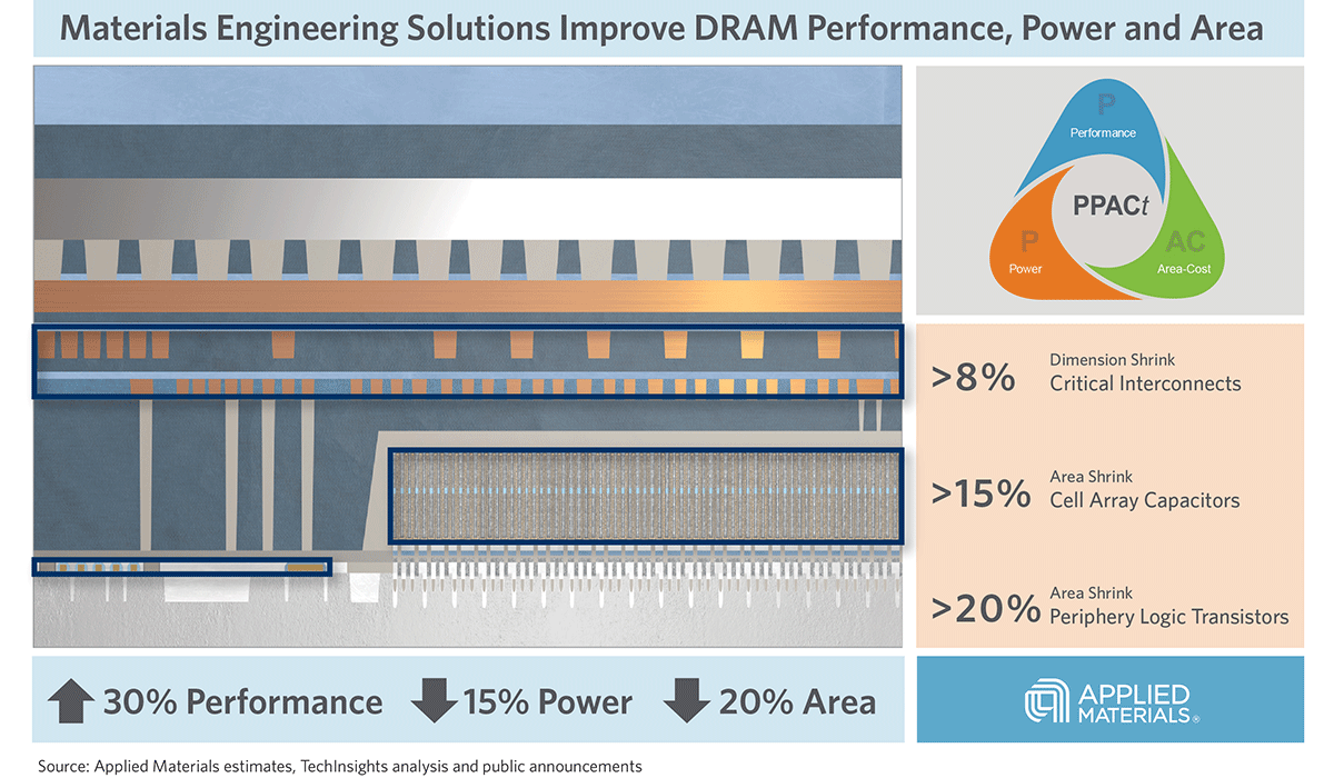
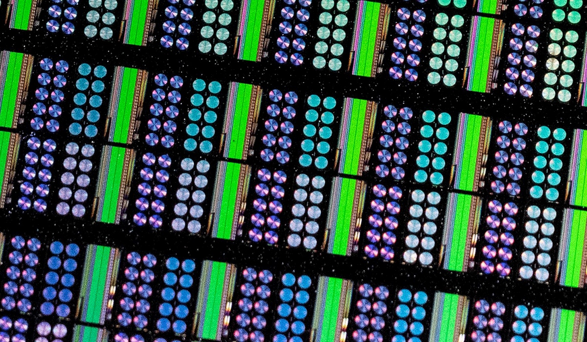
Introducing Breakthroughs in Materials Engineering for DRAM Scaling
To help the industry meet global demand for more affordable, high-performance memory, Applied Materials today introduced solutions that support three levers of DRAM scaling.