Products & Technologies
Products & Services
Contact
Products & Services
Products & Technologies
Services
Resources
Contact
Posted
May 05, 2021

Stay updated on our content.
Introducing Breakthroughs in Materials Engineering for DRAM Scaling
May 05, 2021
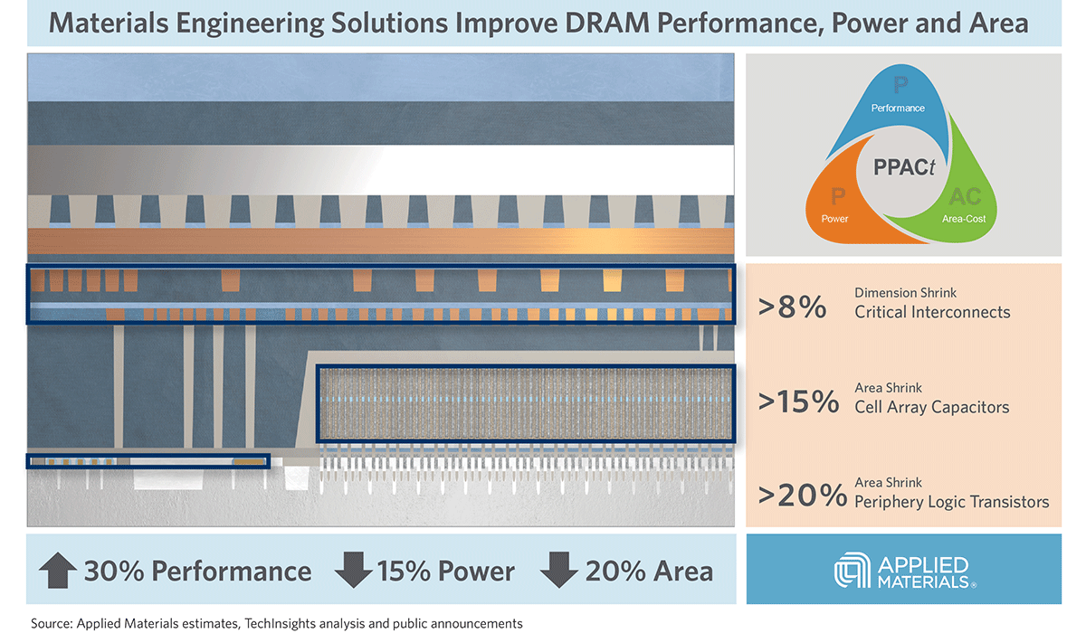
As I described in my last blog, at a time when demand for lower-cost, higher-density DRAM has never been greater, physical limitations are impeding DRAM performance, power, area and cost (PPAC). Without a solution, the unprecedented growth in DRAM capacities that we’ve enjoyed for the past 20 years could be significantly curtailed and slow advances in areas including artificial intelligence and high-performance computing.
To address this challenge, Applied Materials is working with its DRAM customers on materials engineering solutions that create new ways to shrink as well as improve performance and power. Today we announced solutions that support three key levers of DRAM scaling: a new hard mask material for the cell array capacitors, a low-k dielectric material for the interconnect wiring, and the adoption of high-k metal gate (HKMG) transistors in the periphery logic of the chip.
New Draco™ Hard Mask Material Extends DRAM Capacitor Scaling
A common approach to DRAM scaling is to shrink the capacitor’s diameter which causes the aspect ratio to increase in order to maintain adequate surface area and charge. This presents a challenge to DRAM scaling as the etch process needed to create the deep capacitor holes threatens to exceed the limits of the hard mask material that acts as a stencil to determine where each cylinder is placed. As high-energy ions etch the holes, they also eat away at the hard mask. If the hard mask erodes before the capacitor hole is fully formed, the pattern is ruined. Making the hard masks taller is also problematic because it leads to higher aspect ratios as well as the accumulation of etch byproducts in the capacitor holes which causes twisting, bending, under-etch and other killer defects.
To solve this challenge, Applied Materials developed a new hard mask material that is harder and denser than conventional masks. The new Draco™ hard mask increases etch selectivity by more than 30 percent which enables a shorter mask (see Figure 1). We co-optimized the Draco hard mask material to work with our Sym3® Y etch system in a process monitored by the PROVision® eBeam metrology and inspection system that can take nearly half a million measurements per hour. This co-optimization includes advanced RF pulsing which alternates between etching and byproduct removal to enable patterning holes that are perfectly cylindrical, straight and uniform. This is critical to reducing variability in capacitor formation, which is one of the biggest challenges in DRAM scaling. In addition, the Draco hard mask has been engineered to produce volatile byproduct material that doesn’t stick to the walls of the capacitor cylinder and can be much more easily removed than conventional hard masks—even under aggressive etch conditions.
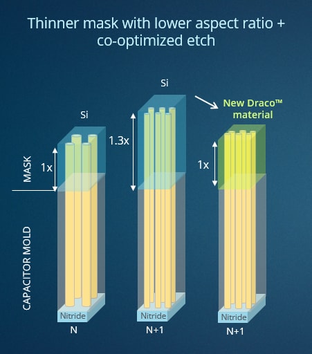
Figure 1: Applied Materials’ Draco hard mask increases etch selectivity by more than 30% which enables a shorter mask.
Further benefits come from the PROVision eBeam system’s ability to gather massive amounts of data that provide actionable insights on hard mask uniformity which is the key to capacitor uniformity. Our solution provides customers with a 50-percent improvement in local critical dimension uniformity and reduces bridge defects by 100X, thereby increasing yields (see Figure 2).
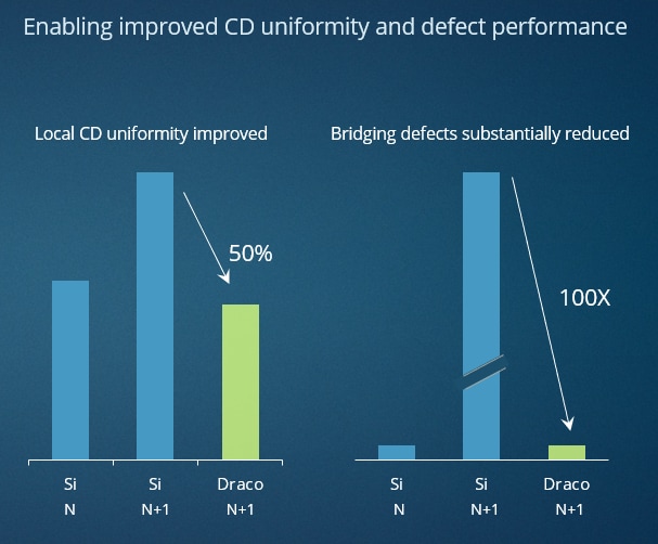
Figure 2: The Draco hard mask helps increase DRAM yield by improving critical dimension (CD) uniformity and reducing bridge defects.
Two other levers of DRAM scaling are related to reducing the peripheral circuitry area which consists of the logic transistors and interconnect wiring that surrounds the DRAM cell array. The performance of the logic transistors must be improved to avoid leakage while the distance between interconnect wiring must be reduced to increase DRAM density. Applied Materials is helping our customers develop solutions for both.
Bringing Black Diamond® Low-k Dielectric to the DRAM Market
Each of the metal lines in the interconnect wiring are surrounded by an insulating dielectric material that prevents interference between signals. Thinning the dielectric layers has reduced DRAM die sizes but caused a new technology challenge: the dielectrics are now too thin to prevent capacitive coupling in the metal lines whereby signals interfere with one another, causing higher power consumption, slower performance, increased heat and reliability risks.
The conventional approach for the better part of 25 years has been to use silane or tetraethoxysilane (TEOS) silicon oxides as the dielectric insulator between adjacent metal conducting lines. Applied recognized that these silicon-oxide films have reached their limit and that the industry needs a lower-capacitance dielectric material that allows DRAM conductive lines to be placed closer together without causing signal interference.
This led us to explore using Applied’s Black Diamond® low-k dielectric material in the DRAM market. Black Diamond is a material Applied first introduced for advanced logic to solve similar scaling challenges. Using carbon as a dopant, the Black Diamond dielectric material enables smaller, more compact interconnect wires that can move signals through DRAM at multi-gigahertz speeds while lowering capacitance, power consumption and crosstalk. To achieve seamless integration into customer process flows, the low-k material also provides excellent interfacial control and adhesion to the incoming layer. We are already working with customers on a new version of Black Diamond for use with future generations of DRAM.
High-k Metal Gate Transistors Bring PPAC Improvements to DRAM
The transistors in the periphery logic of the DRAM chip drive the input-output (I/O) operations and are critical in providing the performance needed in today’s DDR5 DRAM. Until now, DRAM has used transistors based on polysilicon-oxide. This type of transistor fell out of favor with foundry-logic customers by the 28nm node because extreme thinning of the gate dielectric allowed electrons to leak, adversely impacting power and performance. Logic makers switched to high-k metal gate (HKMG) transistors where the polysilicon was replaced with a metal gate and the dielectric was changed to hafnium oxide, a material that improves gate capacitance, leakage and performance.
To drive continued improvements in PPAC, memory makers are now introducing HKMG transistors in advanced DRAM designs. Just like in logic, we expect HKMG to increasingly replace polysilicon transistors over time. Applied is helping enable this inflection with our leadership in deposition and film treatment technologies. Our Endura® Avenir™ RFPVD system has become the industry’s preferred solution for manufacturing the complex HKMG stack as it allows in-vacuum processing of adjacent steps. HKMG transistors also benefit from our epitaxial deposition technologies such as Centura® RP Epi along with film treatments including RadOx™ RTP, Radiance® RTP and DPN which are used to fine-tune the transistor characteristics for optimum performance.
Summary
Bringing new materials to chip manufacturing is never easy. They need to drop into existing process flows and must be compatible with upstream and downstream steps. By co-optimizing process interactions between deposition and etch and incorporating our unique metrology techniques, we are accelerating R&D learning cycles and generating better and faster outcomes for our customers.
Applied’s solutions for DRAM scaling are possible thanks to the breadth and depth of our portfolio and our ability to combine these technologies in unique and highly enabling ways. They also represent another chapter in Applied’s PPACt playbook, which is offsetting the slowing of traditional Moore’s Law scaling with new architectures, 3D structures, novel materials and new ways to shrink along with heterogeneous design and advanced packaging. This new playbook for PPACt will help DRAM designers accelerate their product roadmaps and continue serving record global demand for more affordable, high-performance memory.
Tags: DRAM, scaling, PPACt, interconnect, hard mask, etch, new ways to shrink, Draco, Black Diamond, Sym3, PROVision, eBeam, low-k dielectrics, high-k metal gate, HKMG
Sony Varghese
Director, Strategic Marketing

Dr. Sony Varghese is director of strategic marketing for memory in the Semiconductor Products Group at Applied Materials. In this role, he is involved in identifying challenges to future key inflections in the memory industry. Prior to Applied Materials, he worked on developing various memory technologies within the R&D organization at Micron Technologies. Dr. Varghese has over 20 U.S. patents issued or pending in the area of semiconductor processing and integration. He holds a master’s degree in materials engineering from The National Institute of Technology Surathkal in India and a Ph.D. in mechanical and materials engineering from Oklahoma State University.
Now is the Time for Flat Optics
For many centuries, optical technologies have utilized the same principles and components to bend and manipulate light. Now, another strategy to control light—metasurface optics or flat optics—is moving out of academic labs and heading toward commercial viability.
Seeing a Bright Future for Flat Optics
We are at the beginning of a new technological era for the field of optics. To accelerate the commercialization of Flat Optics, a larger collaborative effort is needed to scale the technology and deliver its full benefits to a wide range of applications.

DRAM Scaling Requires New Materials Engineering Solutions
The AI Era of computing is fueling exponential growth in data generation, and the entire technology ecosystem depends on the semiconductor industry finding new ways to scale DRAM architectures to keep pace with bit demand.