Products & Technologies
Products & Services
Contact
Products & Services
Products & Technologies
Services
Resources
Contact
Posted
April 03, 2021

Stay updated on our content.
Taking a Second Look at “AI”

Apr 03, 2021
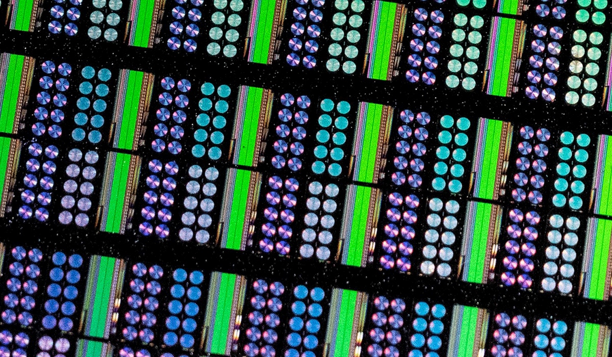
Applied Materials technology has long been used by our customers to build the chips that AI runs on. Last month, we revealed how AI is becoming a highly enabling new ingredient within the solutions we provide to our customers. Our ExtractAI™ technology provides a real-time, intelligent link between our Enlight® optical wafer inspection system and our industry-leading eBeam review system, SEMVision®, allowing the power of adaptive AI-based pattern recognition to be used to give process engineers “Actionable Insights” about yield-killing defects.
What my colleagues in the Process Diagnostics and Control group have accomplished is amazing, but it’s just the beginning of new Big Data and AI capabilities we’re creating at Applied. I’ve spent most of my career working in process R&D, helping our customers develop the new recipes that will eventually run in their fabs. The introduction of ExtractAI technology is a great example of the journey we’ve started toward a new semiconductor industry that fully embraces AI to create AI.
The term AI deserves a second look. “Artificial Intelligence” describes recreating human intelligence, a concept that’s decades old and not particularly consistent with the practical applications of AI today. People are deploying machine learning and AI for pattern recognition to solve real-world problems—not to match wits with humans. While AI can help turn data into useful information, it’s still human intelligence that provides context and turns new insights into better outcomes. I think the semiconductor industry should let AI stand for “Actionable Insights.” We need actionable insights more than ever before.
Ready, Set, Go
How do you bring a new process recipe from R&D to high-volume production? Ideally, as quickly as possible and with the widest margin of error. The stakes are huge, not only for semiconductor manufacturers investing $8 to $18 billion dollars to equip a new 100K wafer starts per month fab, but also for the entire technology ecosystem downstream. How difficult is the challenge? Let’s use board games to make an analogy. Game complexity increases exponentially with the size of the board, the number of different kinds of pieces, and the variety of moves that can be made. Checkers is much easier than Chess, where the number of moves possible exceeds the number of atoms in the known universe. The game of Go is harder still. How is AI doing in these endeavors? In 1994, a Checkers program called Chinook triumphed over the unbeatable Marion Tinsley. In 1997, Garry Kasparov was crushed by IBM’s Deep Blue. And in 2016, over 100 million people watched as Google’s AlphaGo beat Lee Sedol in 4 of 5 matches.
Why did it take AI longer to conquer Go than graduate from Checkers to Chess? Because Go involves a much larger solution space. The board has a 19 by 19 grid of 361 squares and an equivalent number of black and white stones. After the first two moves, there are close to 130,000 possible next moves. How long will it take for AI to learn how to make the process recipes needed to make new chips for even better AI? I won’t hold my breath waiting on that development. Here’s why.
Our process systems are capable of 10,000 combinations, and integrated processes like the ones used to build chip interconnect wiring offer a million combinations. The exotic materials created by these processes can be exceedingly delicate, and exposure to air or wait times between processes can quickly change their properties. Etch processes have more than 100 process control knobs. High voltages pulse through the chambers, and components are eroded with use, which means the conditions are changing in real time. Applied’s process systems use hundreds of sensors to monitor these changing conditions, generating over 1,000 terabytes of data per year. How does process technology compare to board games? I imagine a game of 3-dimensional Go, with multiple colors of stones, and a board that changes its shape with every move!
The point is that developing, transferring and ramping new process recipes is not systematic enough for AI to give us the answers. But given the high stakes, now is the right time to begin to collect Big Data and apply AI pattern recognition to help us find new and “Actionable Insights” that can help engineers accelerate development, reduce risk and maximize the return on investment.
Big Data Creates the Big Picture
The most valuable outcomes will come from thinking holistically, deploying AI from R&D to ramp and high-volume manufacturing. We’ll need data—a lot of it—not just from one process step, but from many steps. Not just from one system, but from fleets of systems. We can do this by incorporating electronic ears, eyes and brains: sensors, imaging and algorithms.
Already, our process systems are loaded with sensors. Our eBeam systems are also capable of collecting petabytes of data from wafers. In fact, we may already have too much data—just not enough “Actionable Insights.” What we do need is a framework for making sense of the data. To find the needles in the haystack that can tell us what to do to tune the recipes to improve PPAC—faster and more repeatably—from lab to fab.
Over time we’ll move to a world of simulations where we can try, fail, try again and improve—well before we invest time and money—and water and energy—to run wafers.
The ideal solution would establish an ecosystem for process development that stretches from R&D to high-volume manufacturing and evolves as new process technologies come into play. The R&D engineer needs a digital design of experiments environment that accelerates the development of new materials and structures, integrates them into existing process flows, widens process margins and reduces variability; it’s about solving problems of time to market for a new generation of technology. The production engineer is solving problems of yield and cost reduction. AI should augment the knowledge and intuition of both by converting actionable data into Actionable Insights—to deliver better results faster.
With ExtractAI technology, Applied made its opening move in a new game of using AI to give customers “Actionable Insights.” There are more moves to play.
Tags: ExtractAI, Enlight, SEMVision, eBeam, Big Data, AI, Actionable Insights
Dr. Raman Achutharaman
Group Vice President and General Manager, Etch and Selective Products Business Unit

Dr. Raman Achutharaman leads the Semiconductor Products Group in defining the technology roadmap; developing the strategic plan to strengthen Applied’s leadership in core wafer fabrication equipment markets; and communicating the vision, strategy, and success to stakeholders. Previously, as general manager of the Etch and Selective Products business unit, he led development and commercialization of the Sym3 Etch system that grew etch revenue from less than $400M to over $2B and gained more than 15 pts of conductor etch market share. Earlier, as general manager of the RTP group, he led development of the Vantage Radiance system, the basis of Applied’s leadership in thermal processing. He received his undergraduate degree in metallurgical engineering from the Indian Institute of Technology, Chennai, and his Ph.D. in materials science and engineering from the University of Minnesota.
Now is the Time for Flat Optics
For many centuries, optical technologies have utilized the same principles and components to bend and manipulate light. Now, another strategy to control light—metasurface optics or flat optics—is moving out of academic labs and heading toward commercial viability.
Seeing a Bright Future for Flat Optics
We are at the beginning of a new technological era for the field of optics. To accelerate the commercialization of Flat Optics, a larger collaborative effort is needed to scale the technology and deliver its full benefits to a wide range of applications.
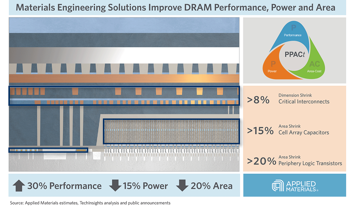
Introducing Breakthroughs in Materials Engineering for DRAM Scaling
To help the industry meet global demand for more affordable, high-performance memory, Applied Materials today introduced solutions that support three levers of DRAM scaling.