Products & Technologies
Products & Technologies
Services
Resources
Posted
March 16, 2021

Stay updated on our content.
Introducing a New Playbook in Process Control

Mar 16, 2021
Time to yield is everything in the semiconductor industry. It means revenue and profit for chipmakers and their customers. It’s also the basis of the entire technology value chain, from the edge to the cloud.
Everyone has a stake in this multibillion-dollar race to high yields. The faster a new technology process node can be proven out and ramped into high-volume manufacturing, the healthier the entire technology ecosystem is.
In this blog series, we’ve been talking about the challenges facing the semiconductor industry when it comes to defect detection and process control. The legacy approach is not keeping up with the complexity of modern semiconductor processes and devices. The industry is not inspecting often enough because of rising cost pressures. Fab engineers filter inspection data to reduce the amount of false positives but wind up missing killer defects and losing precious time.
The situation is unsustainable. The industry needs a breakthrough.
Applied Materials is solving these challenges with a new playbook for process control designed to bring the benefits of Big Data and AI technology to the core of chipmaking technology. Applied’s solution, unveiled today, consists of three elements that work together in real time to find and classify defects faster, better and more cost effectively than legacy approaches. The three elements are:
New Enlight® Optical Wafer Inspection System: in development for five years, the Enlight system combines industry-leading speed with high resolution and advanced optics to collect more yield-critical data per scan. The Enlight system architecture improves the economics of optical inspection, resulting in a 3X reduction in the cost of capturing critical defects as compared to competing approaches. By dramatically improving cost, the Enlight system allows chipmakers to insert many more inspection points in the process flow. The resulting availability of Big Data enhances “line monitoring,” statistical process control methods that can predict yield excursions before they occur, immediately detect excursions so that wafer processing can be halted to protect yields and enable root-cause traceback to accelerate corrective actions and the return to high-volume manufacturing.
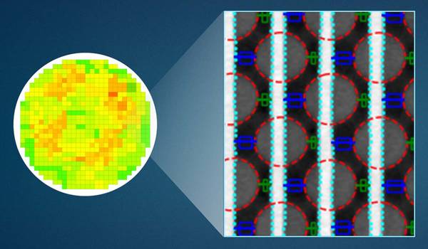
New ExtractAI™ Technology: developed by Applied’s data scientists, ExtractAI technology solves the most difficult problem of wafer inspection—the ability to quickly and accurately distinguish yield-killing defects from the millions of nuisance signals or “noise” generated by high-end optical scanners. ExtractAI is the only solution in the industry that creates a real-time connection between the Big Data generated by the optical inspection system and the eBeam review system that classifies specific yield signals so that by inference, the Enlight system resolves all of the signals on the wafer map, differentiating yield killers from noise. ExtractAI technology is incredibly efficient; it characterizes all of the potential defects on the wafer map after reviewing only 0.001X of the samples. The result is an actionable map of classified defects that accelerates semiconductor node development, ramp and yield. The AI technology is adaptive and quickly identifies new defects during high-volume production while progressively improving its performance and effectiveness as more wafers are scanned.
SEMVision® eBeam Review System: the SEMVision system is the most advanced and widely used eBeam review technology in the world. With its industry-leading resolution, the SEMVision system trains the Enlight system with ExtractAI technology to classify yield-killing defects and distinguish defects from noise. By working together in real time, the Enlight system, ExtractAI technology and SEMVision system help customers identify new defects as they are introduced in the manufacturing flow, enabling higher yields and profitability. The large installed base of SEMVision G7 systems is already compatible with the new Enlight system and ExtractAI technology.
As shown in the animation below, Applied’s innovative solution is the only inspection and review technology that learns and adapts in real time, providing a full wafer map that is fully classified and completely noise free.

With Applied’s unique solution, semiconductor manufacturers can inspect more to gather more data about the health of their process recipe without being overwhelmed by noise. The result is a dramatic acceleration in R&D, ramp and high-volume yield.
Applied has long focused on ensuring continued advancements in the semiconductor industry’s ultimate goal: PPAC, shorthand for improvements in performance, power, and area/cost. In a world rushing to a future in which AI creates trillions of dollars in economic value, time to market has become an even more important factor: the Enlight system with ExtractAI technology delivers the “t” in “PPACt,” the enablement of which is the guiding strategy of Applied Materials.
Applied Materials CEO Gary Dickerson has said that AI will transform every sector of the economy—including the semiconductor industry. With our new playbook for process control, we are now using AI to make the chips that enable better AI.
Tags: Enlight, ExtractAI, SEMVision, AI, Process Control, inspection, Review Defects, New Playbook, Big Data
Oren Faigenzvaig
Product Marketing Head, Optical Defect Control Division

Oren Faigenzvaig is a product marketing head in the optical defect control division at Applied Materials. He joined Applied in 2011 and holds a B.Sc in Electrical and Computer Engineering and MBA in Management of Technology and Innovation from Tel Aviv University.

Adding Sustainability to the Definition of Fab Performance
To enable a more sustainable semiconductor industry, new fabs must be designed to maximize output while reducing energy consumption and emissions. In this blog post, I examine Applied Materials’ efforts to drive fab sustainability through the process equipment we develop for chipmakers. It all starts with an evolution in the mindset of how these systems are designed.

Innovations in eBeam Metrology Enable a New Playbook for Patterning Control
The patterning challenges of today’s most advanced logic and memory chips can be solved with a new playbook that takes the industry from optical target-based approximation to actual, on-device measurements; limited statistical sampling to massive, across-wafer sampling; and single-layer patterning control to integrative multi-layer control. Applied’s new PROVision® 3E system is designed to enable this new playbook.

Breakthrough in Metrology Needed for Patterning Advanced Logic and Memory Chips
As the semiconductor industry increasingly moves from simple 2D chip designs to complex 3D designs based on multipatterning and EUV, patterning control has reached an inflection point. The optical overlay tools and techniques the semiconductor industry traditionally used to reduce errors are simply not precise enough for today’s leading-edge logic and memory chips.
