Products & Technologies
Products & Technologies
Services
Resources
Posted
March 08, 2021

Stay updated on our content.
It’s Time for a New Playbook for Finding and Correcting Defects in Advanced Chips

by Ortal Yesodi
Mar 08, 2021
Semiconductors are the foundation of all technology inflections. The PC Era was ushered in by powerful microprocessors. The Mobile Era by advances that put high-performance, low-power chips in smartphones. The Cloud Era with processors and banks of memory and storage in huge data centers. While these markets remain large and growing, we are now entering the AI Era fueled by the Internet of Things (IoT), Big Data and 5G, shaped by new types of computing architectures and chip designs. Semiconductor progress has never been more critical to the growth of the global economy.
The stakes are high if we cannot continue to advance the semiconductor technology roadmap with high-performance logic and memory devices in the enormous volumes required for this new era. Getting from R&D to high-volume manufacturing of new technology nodes is a complex process gated primarily by the ability to detect and correct defects. The methods used by the industry to perform defect inspection and review have remained relatively the same for decades. Is it time to rethink our approaches?
This is the first blog in a series examining challenges around defect detection and correction. Any obstacles to advancement in the semiconductor industry ripple forward into the much larger global electronics ecosystem. The faster those obstacles can be overcome, the faster the world moves forward. Time is a critical factor.
Time is Money
Given the extraordinary cost of being in the semiconductor industry, its business imperatives revolve around time: time to development, time to volume production, time to market, and time to revenue. And the most critical parameter is time to yield. Even a small acceleration in the time it takes to get from R&D of new processes to the early ramp phase and then to high-volume manufacturing equates to billions of dollars in value for chipmakers (see Figure 1).

Figure 1: Even a slight shift to the left in the yield curve (achieving high-volume manufacturing faster) can be worth billions.
The opposite is also true, of course. Delays in yield improvement cost time, money and market share in the new computing era which fuels the most valuable businesses the world has ever seen.
Chip Complexity
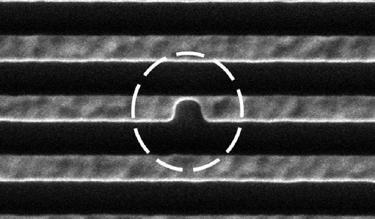
Defect detection is the gating factor in yield improvement. The faster yield-killing defects can be found, the faster they can be corrected. However, defects are getting harder to find. For example, ever-smaller line widths turn tiny nuisance particles into yield-killers. When building sophisticated 3D transistors, and when executing complex multi-patterning steps, small variances can multiply to produce yield-killing defects. This further complicates matters because a defect can be revealed long after its root cause occurred: every subsequent process step following the introduction of the defect is time and money wasted.
As the complexity of chips is rising and defects are becoming increasingly difficult to find, the industry should be inspecting more. But in reality, the exact opposite is happening—inspection steps are being limited. Why is that?
Economic Challenges
The fab economic model becomes a major challenge at this juncture. For every nanometer of advancement, the number of wafer processing steps grows rapidly. More steps to inspect equals more inspection cost. Additionally, the increasing sophistication of the optical scanners used to find defects has increased their cost as well. More cost per scanner equals more cost per wafer scan (see Figure 2).
.png)
Figure 2: An increase in process steps—and optical inspection system complexity and cost—are resulting in an unsustainable increase in wafer inspection cost.
As a result, engineers are inspecting at fewer steps than they would like simply to keep their process control budgets from skyrocketing. Of course, limiting the number of inspection steps results in less of the data needed to accelerate defect detection, traceback, root cause analysis and correction—and thereby accelerate time to yield. Yet, these inspection costs are very real and cannot be wished away. The number of inspection steps inserted into the process recipe is one of the few points of cost control available. Fabs budget a certain amount of inspection dollars, engineers gather as much data as they can afford, and everyone hopes for the best.
The inspection paradigm used today was developed in a very different time. Not only was Moore’s Law operating on schedule, defects that were mere nuisance blips on a wafer map in previous generations are now yield killers. The reality is that the industry is inspecting less and therefore collecting less data—relative to the soaring complexity of the challenge—precisely when we should be inspecting more. What we need is a new playbook for process control that can accelerate time to yield without breaking the fab economic model. This is an innovation imperative for the semiconductor industry.
In my next blog, I’ll describe the breakthroughs needed to revolutionize defect detection and correction in the AI Era.
Tags: Process Control, inspection, Review, Defects, New Playbook
Ortal Yesodi
Product Marketing Manager, Process Diagnostics and Control Group

Ortal Yesodi is a product marketing manager in the Process Diagnostics and Control group at Applied Materials. She joined Applied in 2013 and holds a bachelor’s degree in electrical and computer engineering from Ben Gurion University of the Negev.

Adding Sustainability to the Definition of Fab Performance
To enable a more sustainable semiconductor industry, new fabs must be designed to maximize output while reducing energy consumption and emissions. In this blog post, I examine Applied Materials’ efforts to drive fab sustainability through the process equipment we develop for chipmakers. It all starts with an evolution in the mindset of how these systems are designed.

Innovations in eBeam Metrology Enable a New Playbook for Patterning Control
The patterning challenges of today’s most advanced logic and memory chips can be solved with a new playbook that takes the industry from optical target-based approximation to actual, on-device measurements; limited statistical sampling to massive, across-wafer sampling; and single-layer patterning control to integrative multi-layer control. Applied’s new PROVision® 3E system is designed to enable this new playbook.

Breakthrough in Metrology Needed for Patterning Advanced Logic and Memory Chips
As the semiconductor industry increasingly moves from simple 2D chip designs to complex 3D designs based on multipatterning and EUV, patterning control has reached an inflection point. The optical overlay tools and techniques the semiconductor industry traditionally used to reduce errors are simply not precise enough for today’s leading-edge logic and memory chips.
