Products & Technologies
Products & Services
Contact
Products & Services
Products & Technologies
Services
Resources
Contact
Posted
October 18, 2021

Stay updated on our content.
Innovations in eBeam Metrology Enable a New Playbook for Patterning Control
Oct 18, 2021
The semiconductor industry is changing. We see it everywhere. Plans are in place for the largest fab capacity expansions in decades. Classic Moore’s Law scaling no longer functions like clockwork. Cloud service providers are now designing many of their own chips. These macro changes overshadow the more intricate technological changes in the fab, but they are all part of the same industry in transition to the future.
You can’t make tomorrow’s leading-edge chips with yesterday’s fab processes. My previous blog highlighted a major inflection in patterning control as the traditional optical overlay tools and techniques the semiconductor industry has used for decades to reduce alignment errors are no longer precise enough for the next generation of advanced logic and memory chips. To put it bluntly: you can’t fix what you can’t measure, and you can’t measure what you can’t see. The industry needs a breakthrough in metrology to enable the best chip performance, power, area and cost—and accelerate time to market (PPACt™).
Today, Applied Materials is introducing a new playbook for patterning control that is anchored by our latest innovation in eBeam metrology—the PROVision® 3E system. The unique technical features of the system enable the industry to move from:
- Optical target-based approximation to actual, on-device metrology
- Limited statistical sampling to massive, across-wafer sampling
- Single-layer control to 3D integrative multi-layer control
If You Can’t See It, You Can’t Align It
The PROVision 3E system helps customers solve the incredible challenge of aligning the billions of features that make up the critical layers of advanced chips. Following generations of feature size reductions, the adoption of multipatterning, and the introduction of tall 3D structures that cause interlayer stresses and distortions, the tolerances for placement errors have all but vanished.
The mask-oriented, optical techniques that have long been used to ensure alignment simply aren’t able to see, diagnose and remedy the placement errors that occur once chipmakers commit to etching intended patterns into expensive wafers. The inability to quickly identify and fix placement errors slows process R&D and time to market.
A Breakthrough in Metrology for a New Playbook
The PROVision 3E system provides the industry’s best-ever combination of resolution, measurement accuracy, speed and through-layer imaging to enable a new playbook for patterning control.
First, engineers can transition from optical target-based approximation to actual, on-device measurement, taking advantage of the PROVision 3E system’s nanometer resolution which can take discrete measurements down to a specific gate—and the decades of CD SEM industry experience that are reflected in the new system’s architecture.
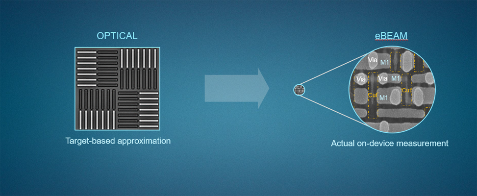
Figure 1: From optical target-based approximation to actual, on-device measurements.
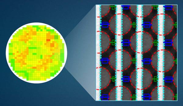
Second, engineers can move from limited statistical sampling to massive, across-wafer sampling, using the speed of the PROVision 3E system which produces 10 million accurate, actionable measurements per hour. Massive sampling reveals “process signatures,” variation issues related to specific process steps that engineers can remedy.
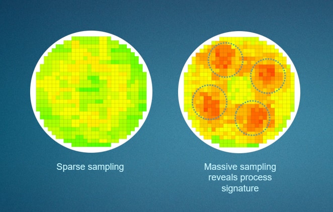
Figure 2: From limited statistical sampling to massive, across-wafer sampling.
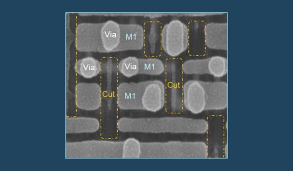
Third, engineers can advance from single-layer patterning control to integrative multi-layer control. The “E” in PROVision 3E stands for Applied’s Elluminator® technology which efficiently collects high-energy back-scattered electrons to quickly image and measure critical dimensions and edge placement in multiple layers of the wafer simultaneously.
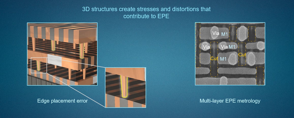
Figure 3: Integrative multi-layer control.
Already at Work, Measuring the Future
Officially launched today, the PROVision 3E system is already being used by our leading foundry-logic, DRAM and NAND customers worldwide.
The PROVision 3E system is also a key component of Applied’s AIx™(Actionable Insight Accelerator) platform which helps customers accelerate development of new chip technologies throughout every step of the journey—from R&D to ramp and high-volume manufacturing (see Figure 4). The key is the PROVision 3E system’s ability to generate massive amounts of data through its incredible resolution, speed and multi-layer measurement capability. This feeds the AIx analytics platform with actionable data that provides engineers with the actionable insights they need to accelerate process development.
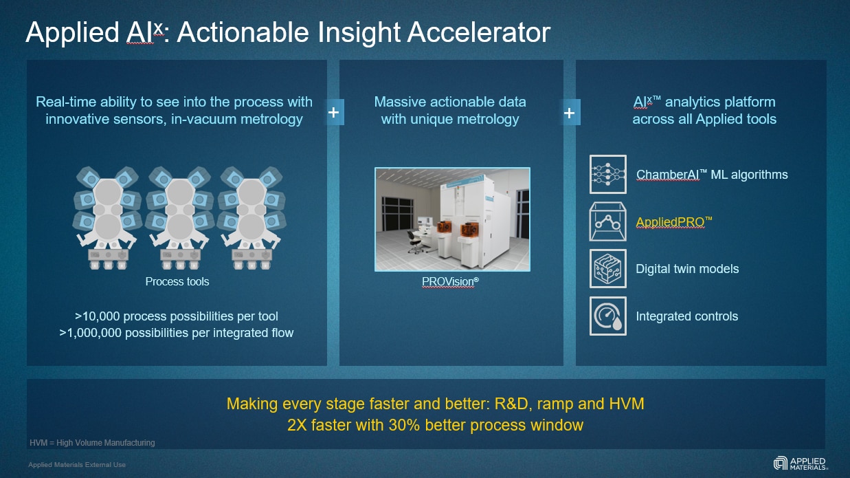
Figure 4: The PROVision 3E system is a key component of Applied’s AIx platform which combines process technology, sensors, metrology and data analytics to accelerate process development from R&D to ramp and high-volume manufacturing.
The PROVision 3E system exemplifies how eBeam technology can be used by customers to overcome complexity and accelerate R&D and time to market. Check out Applied’s 2021 Process Control and AppliedPRO™ Master Class to learn more.
Tags: Patterning, Process Control, PROVision, metrology, EUV, 3D, AIx, PPACt, New Playbook
Maayan Bar-Zvi
Patterning Division - Process Diagnostics and Control (PDC) group

Maayan Bar-Zvi manages the Patterning Division of Applied Materials’ Process Diagnostics and Control (PDC) group, including eBeam metrology and next-generation process control products and solutions. He has held several leadership positions during his 18 years with the PDC group, including Application Technology Manager, Product Manager and Product Line Head. Maayan earned a B.S. in engineering from Tel-Aviv University.

Adding Sustainability to the Definition of Fab Performance
To enable a more sustainable semiconductor industry, new fabs must be designed to maximize output while reducing energy consumption and emissions. In this blog post, I examine Applied Materials’ efforts to drive fab sustainability through the process equipment we develop for chipmakers. It all starts with an evolution in the mindset of how these systems are designed.
Breakthrough in Metrology Needed for Patterning Advanced Logic and Memory Chips
As the semiconductor industry increasingly moves from simple 2D chip designs to complex 3D designs based on multipatterning and EUV, patterning control has reached an inflection point. The optical overlay tools and techniques the semiconductor industry traditionally used to reduce errors are simply not precise enough for today’s leading-edge logic and memory chips.

The Fourth Era of Computing Needs More than Advanced Logic and Memory Chips
At the Applied Materials Master Class today, we highlight two fast-growing and highly enabling areas of the semiconductor industry. “ICAPS” silicon powers billions of new devices on the edge—including electric vehicles. No longer an afterthought, packaging now enables the benefits associated with Moore’s Law to continue even as 2D scaling slows. Today’s class demonstrates that the AI Era requires innovation across a wide range of technologies, from the edge to the cloud.