Products & Technologies
Products & Services
Contact
Products & Services
Products & Technologies
Services
Resources
Contact
Posted
October 13, 2021

Stay updated on our content.
Breakthrough in Metrology Needed for Patterning Advanced Logic and Memory Chips
Oct 13, 2021
An old axiom of business management asserts that “what gets measured, gets managed.” Metrology—the scientific study of measurement—is effective when data is readily available and consistent. That’s not always the case in the semiconductor world, however. What happens when the things you’re trying to measure so radically change that the metrology is no longer effective? And what if you don’t discover the metrology shortcomings until you’re faced with inexplicable yield issues and start falling behind? These are big questions in the industry today.
Semiconductor production is an extremely expensive and complicated endeavor. The journey from R&D to high-volume manufacturing is actually a race. Whoever gets there first wins competitive advantage in terms of revenue, market share and profitability. Metrology has always been critical to controlling and perfecting the chipmaking process. However, the chip structures are now so small and complex that the way we measure needs to evolve.
Patterning Control at a Crossroads
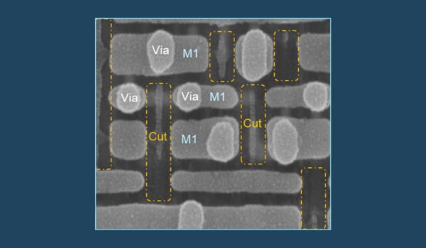
Advanced chips are built up one layer at a time, and each of billions of individual features must be perfectly patterned and aligned to create working transistors and interconnects with the best performance and power characteristics. Patterning errors impact time to market, reduce yields and ultimately slow down an economy that runs on silicon (see Figure 1).
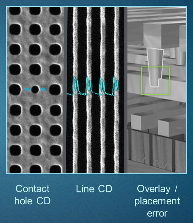
Figure 1: Patterning challenges include variations in the critical dimensions (CD) of contact holes, lines and spaces along with edge placement errors.
As the industry increasingly moves from simple 2D chip designs to complex 3D designs based on multipatterning and EUV, patterning control has reached an inflection point. The optical overlay tools and techniques the semiconductor industry traditionally used to measure alignment are simply not precise enough for today’s leading-edge logic and memory chips.
The incredible precision required to align the many layers of a chip is further complicated by the fact that process conditions vary in different regions of the process chamber. This means the pattern of each die being formed will be slightly different depending on where the die sits on the wafer. So not only does each layer need to align perfectly with what’s above and below it, these alignments need to be made uniform across the wafer so that devices from different areas of the wafer yield and have good electrical characteristics.
Adding to the complexity is the nature of 3D device structures, which require three times the number of measurements compared to planar devices. Taller structures create distortions both locally and between layers. And next-generation gate-all-around transistors will require even more measurements.
It may surprise even some seasoned industry observers to learn that the optical metrology systems used to control overlay in fabs do not have the resolution needed to measure the devices being produced. Instead, these systems take measurements from proxy targets, which are horizontal and vertical marks adjacent to the dies that help optical metrology tools approximate whether the desired patterns are being placed correctly (see Figure 2).
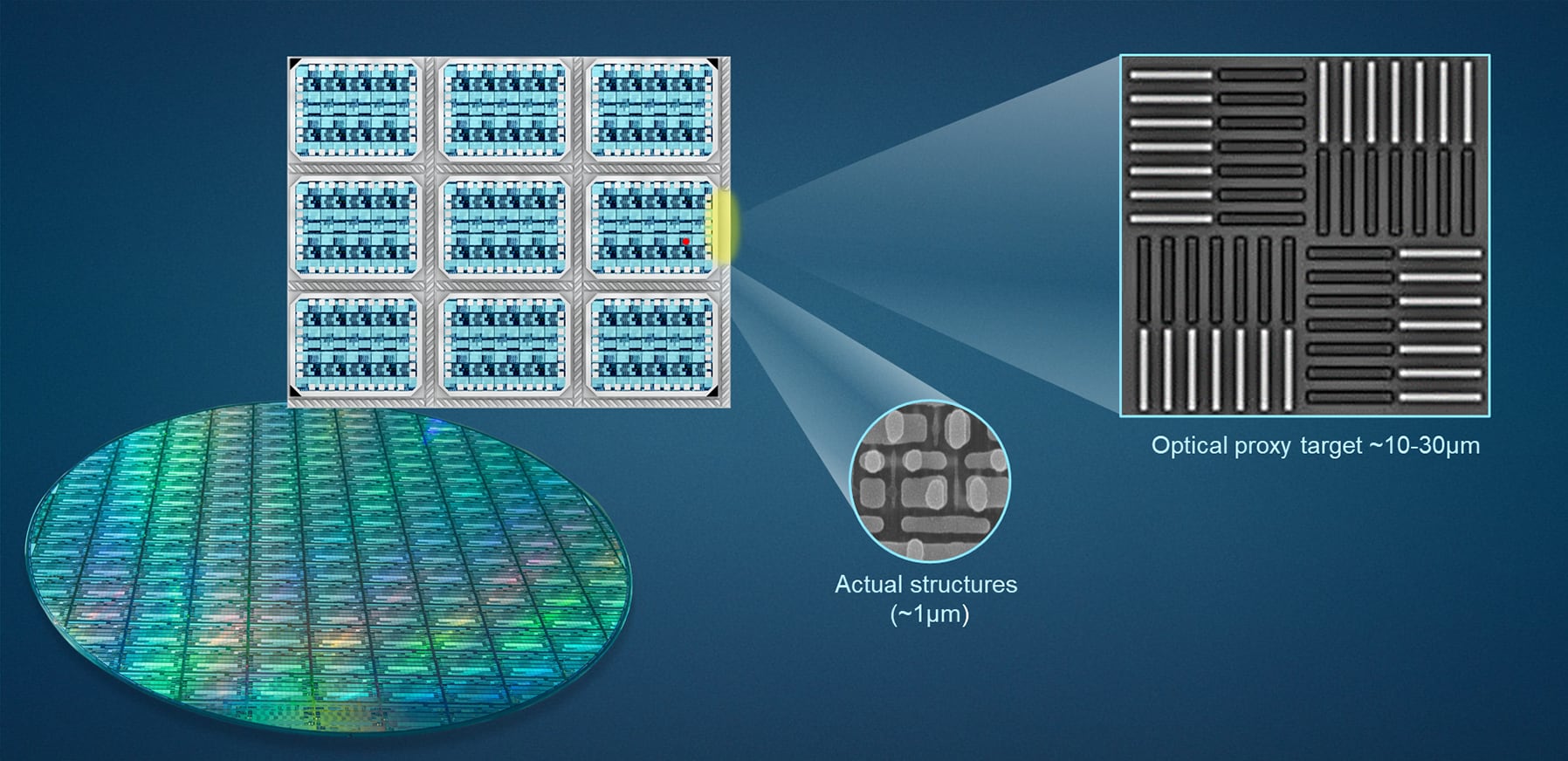
Figure 2: Today’s optical metrology systems rely on proxy targets, which are about 10X larger than the actual on-die features, to estimate if patterns are being placed correctly.
This indirect method of measurement was developed in the days of 2D scaling and single deposition and etch patterning. Process engineers have been using algorithms to compensate for the lack of on-device measurements, but this technique is reaching the limits of its precision—at exactly the time that the tolerance for alignment errors is all but disappearing.
Metrology plays a huge role in speeding processes into high-volume manufacturing and controlling the processes to avoid excursions. Patterning errors result in costs ranging from scrapped wafers to low yields to low pricing from chips that work but have compromised power and performance.
We all want to resolve these issues. But you can’t fix what you can’t measure. And you can’t measure what you can’t see.
Toward a Solution
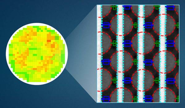
One solution for improving patterning control would be to move from target-based approximations to actual measurements of what’s happening within each die across the entire wafer.
The ideal approach would address more than overlay issues. It would also produce data that could be used to diagnose any issues in all of the process technologies involved, from deposition and etch to thermals and CMP. The ability to conduct massive, across-wafer sampling would enable process engineers to discover and solve process variation issues faster, improve PPAC (power, performance and area-cost) and accelerate “t” (time to yield). Such data could also be used to feed artificial intelligence engines, such as Applied’s innovative AIx™ platform, to further speed the development and commercial deployment of new materials and process technologies.
In my next blog I’ll describe how Applied is enabling a new playbook for patterning control—one that can help chipmakers more precisely measure what’s happening in their advanced processes, so they can better manage the development of new chip designs that will lay the foundation for the industry’s future. Please also mark your calendar for Oct. 18 when Applied will host its 2021 Process Control and AppliedPRO™ Master Class, where we will discuss our latest innovations in process control.
Tags: metrology, Patterning, Process Control, EUV, AIx, PPACt
Maayan Bar-Zvi
Patterning Division - Process Diagnostics and Control (PDC) group

Maayan Bar-Zvi manages the Patterning Division of Applied Materials’ Process Diagnostics and Control (PDC) group, including eBeam metrology and next-generation process control products and solutions. He has held several leadership positions during his 18 years with the PDC group, including Application Technology Manager, Product Manager and Product Line Head. Maayan earned a B.S. in engineering from Tel-Aviv University.

Adding Sustainability to the Definition of Fab Performance
To enable a more sustainable semiconductor industry, new fabs must be designed to maximize output while reducing energy consumption and emissions. In this blog post, I examine Applied Materials’ efforts to drive fab sustainability through the process equipment we develop for chipmakers. It all starts with an evolution in the mindset of how these systems are designed.
Innovations in eBeam Metrology Enable a New Playbook for Patterning Control
The patterning challenges of today’s most advanced logic and memory chips can be solved with a new playbook that takes the industry from optical target-based approximation to actual, on-device measurements; limited statistical sampling to massive, across-wafer sampling; and single-layer patterning control to integrative multi-layer control. Applied’s new PROVision® 3E system is designed to enable this new playbook.

The Fourth Era of Computing Needs More than Advanced Logic and Memory Chips
At the Applied Materials Master Class today, we highlight two fast-growing and highly enabling areas of the semiconductor industry. “ICAPS” silicon powers billions of new devices on the edge—including electric vehicles. No longer an afterthought, packaging now enables the benefits associated with Moore’s Law to continue even as 2D scaling slows. Today’s class demonstrates that the AI Era requires innovation across a wide range of technologies, from the edge to the cloud.