Products & Technologies
Products & Technologies
Services
Resources
Posted
August 19, 2020

Stay updated on our content.
How New Materials and Memories Can Help the AI Ecosystem Bend the Climate Curve
by Ellie Yieh
Aug 19, 2020
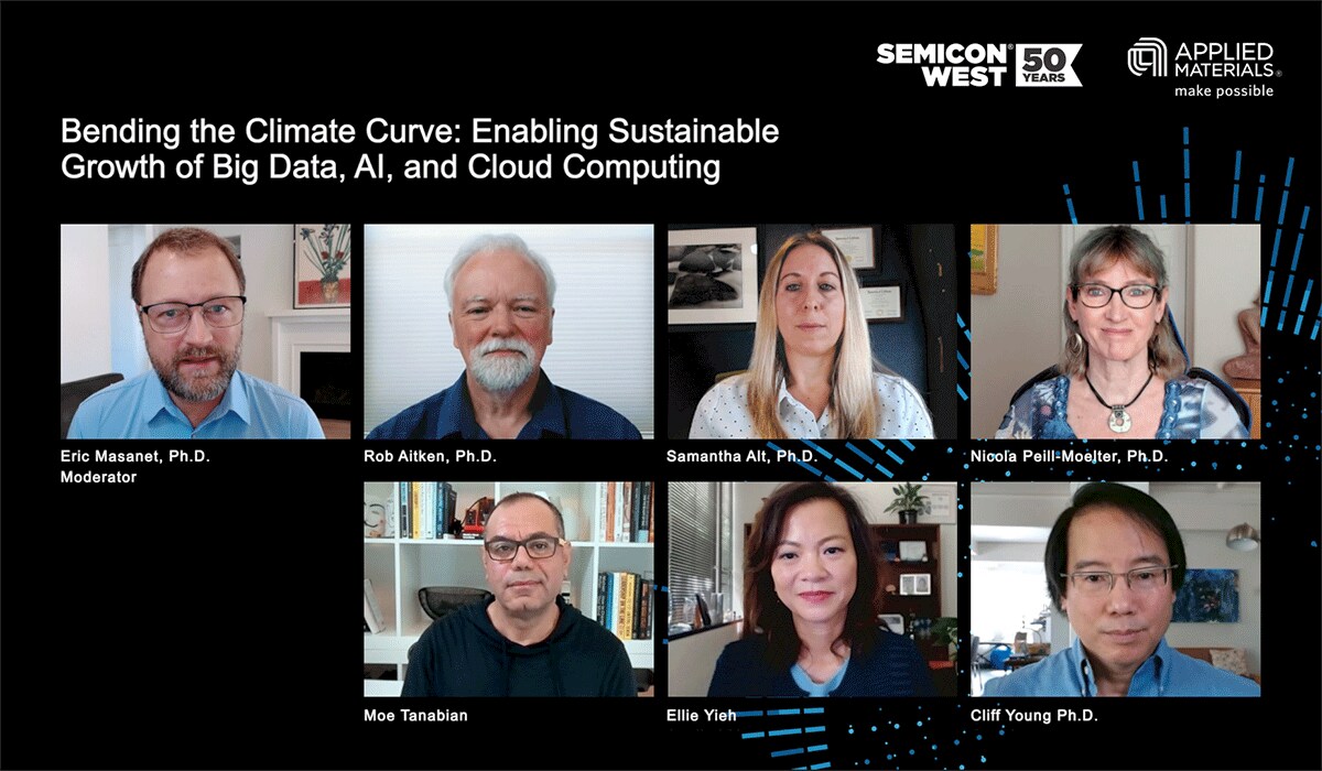
I recently had the honor of participating in a panel discussion titled, “Bending the Climate Curve: Enabling Sustainable Growth of Big Data, AI and Cloud Computing.” It was part of the 50th annual SEMICON West, which was held in a virtual format this year.
Joining me on the panel were industry experts from Arm, Google, Intel, Microsoft, UC Santa Barbara and VMware, and our conversation focused on how technology can be used to help mitigate—rather than contribute to—climate change. As we prepared for the discussion, it became clear that the mass proliferation of Big Data, AI and cloud computing introduces potentially opposing outcomes.
“In one narrative, analysts predict unsustainable growth in IT’s energy use and emissions due to the rise of 5G, the Internet of Things and artificial intelligence,” said panel moderator Dr. Eric Masanet, a UC Santa Barbara professor and a lead author of the UN’s Intergovernmental Panel on Climate Change (IPCC) Sixth Assessment Report. “But there is another narrative in which analysts suggest that the energy efficiency gains made by the IT industry, its adoption of renewable energy, and the emissions savings that IT can bring to other sectors of the economy could, in fact, bend the climate curve.”
As we dug deeper into the question of whether AI and Big Data are environmental saviors or climate change accelerants, my fellow panelists and I focused on a series of emerging innovations with the promise to sharply lower power while still delivering impressive performance gains. At a time when classic Moore’s Law scaling is increasingly challenged and Dennard scaling has effectively ended, Applied Materials is addressing the climate challenge in multiple ways, three of which I outlined during the panel.
One is by improving the eco-performance of our existing and new process systems with hardware and software upgrades that reduce energy use, chemical use and cleanroom space requirements. We call this our “ecoUP” initiative and it includes a “3 by 30” goal for our manufacturing systems: on a per-wafer basis, we are targeting a 30 percent reduction in equivalent energy consumption, a 30 percent reduction in chemical consumption, and a 30 percent increase in throughput density—which is the number of wafers processed per square foot of cleanroom space—by 2030.
We are also accelerating a New Playbook for semiconductor power, performance, area/cost and time to market (PPACt) to ensure improvements across these vectors will continue to be met. One aspect of this playbook is developing new ways for the industry to continue shrinking transistors without compromising power and performance. An example of a recent innovation is our new selective tungsten processing technology that removes a critical bottleneck to continued 2D scaling of transistors in foundry-logic nodes at 5nm, 3nm and below.
A third area where Applied is helping address climate change is by working with our customers and the technology ecosystem to develop new chip architectures that are better suited to the requirements of AI computing, which are markedly different than what defined the PC era.
On the memory front, sustainable AI requires new types of high-performance, low-power, nonvolatile memory that sits closer to the compute engine. This is an emerging market that Applied is helping to enable with our Endura® Clover™ and Endura® Impulse™ PVD systems for MRAM, PCRAM and ReRAM.
“What I would look to for improving our energy efficiency globally in the future would be to improve our memory systems,” said Arm R&D Fellow, Dr. Rob Aitken. “Moving data around is incredibly inefficient. Bringing the compute closer to the memory is the path forward, whether that’s through die stacking or moving AI to the edge or whether it’s through improved memory structures such as MRAM—each of these things have something to contribute.” Rob expands on this point and shares more of his key takeaways in this blog.
Moe Tanabian, General Manager—Intelligent Devices at Microsoft, added “Something that will make a huge difference is lower power, special-purpose chips that are meant for edge AI acceleration—things around sub-100 milliwatts. That will have a major impact on our energy consumption.”
Dr. Cliff Young, Software Engineer at Google, observed, “We’ve been building some of our own chips for neural network applications over the last seven years or so. As part of building them, we’ve been willing to break previous abstractions...We’ve changed mathematics, we’ve changed our networks, we’ve changed the number of cores per chip and many other things which previously might have been set in stone. We’re willing to break abstractions at all levels of the stack.”
The use of nonvolatile, high-density memories can have important system-level benefits, according to Dr. Samantha Alt, a Cloud Solution Architect at Intel. Alt shared that renewable energy sources could be more widely deployed across data centers if there were a means to turn servers on and off based on the availability of clean energy—or what some call “time shifting.” In order to support this, persistent memory is needed to be able to save the state, load it back up and continue executing when the energy becomes available again.
As we moved through our discussion, the biggest takeaway for me was how common our goals are relative to scaling the electronics industry as responsible environmental stewards. The challenge, I believe, is that as we become more specialized, we run the risk of losing important and wide-ranging conversations across multiple industry tiers. We need to facilitate greater collaboration across the ecosystem from Materials to Systems™ and Systems to Materials™ so that our collective knowledge can help “bend the climate curve.”
Intel’s Alt may have summed it up best: “There needs to be much better collaboration between manufacturing, hardware and software. This is where we’re going to gain the most efficiencies, especially in the data center. We all have our expertise and we’re all going to continue to drive innovation in our respective areas, but we need to make sure that all of them are connected together much better than they currently are today.”
A replay of the full panel session is available below and on the Applied Materials YouTube channel.
Tags: SEMICON West, sustainability, Big Data, AI, cloud computing, climate change, Arm, Google, Intel, Microsoft, UC Santa Barbara, VMware
Ellie Yieh
Corporate Vice President, Advanced Product Technology Development

As corporate vice president for Advanced Product Technology Development, Ellie is responsible for Applied’s state-of-the-art Maydan Technology Center and works closely with customers to drive advanced product development and technology roadmaps. In addition, Ellie leads R&D for developing new memory and logic innovations. She received a B.S. in chemical engineering from the University of California, Berkeley and holds more than 100 semiconductor engineering patents. In 2016 she was inducted into the Women in Technology International Hall of Fame for outstanding contributions to scientific and technological communities. She was also named one of the 2015 “Top 50 Most Powerful Women in Technology” by the National Diversity Council. Learn more about Ellie’s career journey in this Nanochip article.

Now is the Time for Flat Optics
For many centuries, optical technologies have utilized the same principles and components to bend and manipulate light. Now, another strategy to control light—metasurface optics or flat optics—is moving out of academic labs and heading toward commercial viability.
Seeing a Bright Future for Flat Optics
We are at the beginning of a new technological era for the field of optics. To accelerate the commercialization of Flat Optics, a larger collaborative effort is needed to scale the technology and deliver its full benefits to a wide range of applications.
Introducing Breakthroughs in Materials Engineering for DRAM Scaling
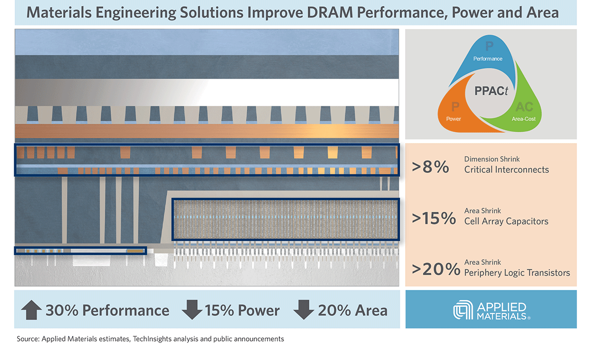
To help the industry meet global demand for more affordable, high-performance memory, Applied Materials today introduced solutions that support three levers of DRAM scaling.
