Products & Technologies
Products & Technologies
Services
Resources
Posted
May 30, 2018

Stay updated on our content.
Final Industry Thoughts on Full-Nodes, Inter-Nodes, Leading-Nodes and Trailing-Nodes - Part 3

May 30, 2018
In part two of this blog series, I provided broader industry context about AI and IoT, and introduced “multicolor” as a 3D technique. I showed that 3D techniques have extended the roadmap in NAND as we now define density not in terms of memory cells per mm2, but in cells per mm3. I described that similar thinking is coming to logic, with transistor features moving vertically into successive layers of the chip. In the final piece of this blog series, I’ll discuss an idea called “integrated materials systems” that Applied’s Prabu Raja introduced at the Industry Strategy Symposium (ISS) panel. First, a brief history of the evolution of materials engineering and a little bit about Prabu’s background.
A Brief History: From Unit Processes and Systems to Integrated Processes and Systems
In the early days of Moore’s Law (Era One), wafers moved from one unit process system to the next, with each individual tool duly performing its task (e.g. deposition, etch, implant and anneal), one material at a time. At 90nm (Era Two), materials engineering became so demanding that chambers for two critical steps – pre-clean and selective epitaxy – were combined into the same platform. A wafer could move from one chamber to the next within the same platform, remaining under vacuum and free of atmospheric contaminants.
Some Background on Prabu Raja
Prabu Raja once led Applied’s PVD business, helping the company build one of the most successful product positions in the industry. In 2012, he took over the etch business and led the development of the Applied Centris™ Sym3™ Etch system, Applied’s fastest-ramping product ever. By the time of the ISS panel, Prabu was responsible for the entire semiconductor equipment business at Applied Materials. The company now develops new products in teams that combine experts in chemistry as well as physics, mechanical engineering and software, including AI. As Moore’s Law slows, such an interdisciplinary approach will be needed to successfully identify, integrate and optimize more materials from the periodic table. The future will be about combining multiple materials in entirely new ways, in an approach Prabu calls “integrated materials systems.”
Armed with this background information, I will now summarize what Prabu said at the ISS panel.
From Bulk Materials to Integrated Materials
The easy days of working with individual materials from the periodic table are over. Continued advances in performance, power and area/cost (PPAC) require “integrated materials” that work together to form novel structures with precise electrical properties. Today, we are working with ten different types of silicon dioxide and eight different types of silicon nitride. At the ultra-nanoscale, materials behave differently: surface properties now dominate the bulk properties we grew up with. Properties such as Surface tension, Capillary action, Wall and Grain boundary scattering all come into play. We need to control and manipulate atoms – in how we assemble them, disassemble them and modify them. Crystal orientation and doping uniformity (of adding measured amounts of one material into another) also become important. Finally, when a group of such nanomaterials are stacked together in one place, the interfaces between them will have a big impact on device performance and need to be engineered carefully at the atomic level.
From Integrated Process Systems to Integrated Materials Systems
Assembling these integrated materials at the atomic scale to achieve predictable properties and interactions is an increasingly complex task that requires multiple process steps to be carried out in a precise arrangement, often within the same platform, and sometimes within a single chamber. Engineering materials in vacuum permits precise engineering of the material-to-material interfaces.
Integrated materials systems will allow designers to make devices they never dreamed possible. Selective processing is a new type of capability where we can selectively deposit or selectively remove only those materials that we want and only where we want them. Etching expands from conventional plasma-based to chemistry-based, offering lateral and even non-line-of-sight removals; deposition and etch will be combined in a single platform; implant will be used for shaping; e-beam inspection will create analytics that can influence the process flow to improve outcomes; and AI will be used to identify unseen relationships between process knobs and outcomes.
New Devices, New Materials, New Collaboration
As I wrote in part two of this blog series, data growth is accelerating just as Moore’s Law is slowing. To realize the promise of the Internet of Things, Big Data and AI, the industry needs new system architectures, new devices and new materials and materials engineering. The industry has an opportunity to collaborate at all levels to speed new materials to market. System architects are looking to break the “memory wall” that forms a bottleneck between processors and storage. New memories like MRAM, PCRAM and Intel® 3D XPoint™ technology aim to improve the connection between logic and memory – while neuromorphic approaches seek to merge the two. These new devices are based on complex multi-materials stacks that need to be precisely deposited and removed to maintain interface quality.
Given the complexity, progress depends on a new level of industry collaboration. Customers are asking for earlier and deeper collaboration: the integrated materials systems era is here. At Applied Materials, we look forward to a renaissance in innovation, from new materials to devices, design techniques and systems.
Intel and 3D XPoint are trademarks of Intel Corporation or its subsidiaries in the U.S. and/or other countries.
Tags: nodes, inter-nodes, leading-nodes, trailing-nodes, ISS, full-nodes, AI, artificial intelligence, materials innovation, iot, materials engineering, 3D NAND, vertical scaling, integrated materials systems, selective processing
Sundeep Bajikar
Corporate Vice President, Corporate Strategy and Marketing

Sundeep is Head of Corporate Strategy and Marketing (CSM) and guides the executive leadership team in the development of the company's growth thesis, strategic priorities, key initiatives and investor communications. He is also responsible for developing Applied’s marketing capabilities and community. Sundeep’s work served as the foundation for Applied’s strategies related to AI, ICAPS, Heterogenous Integration and Net Zero.
He joined Applied in 2017 after spending ten years as a Senior Equity Research Analyst covering global technology stocks, including Apple and Samsung Electronics, for Morgan Stanley and Jefferies. Previously he worked for a decade as a researcher, ASIC design engineer, system architect and strategic planning manager at Intel Corporation.
Sundeep holds an MBA in finance from The Wharton School and M.S. degrees in electrical engineering and mechanical engineering from the University of Minnesota. He holds 13 U.S. and international patents with more than 30 additional patents pending. Sundeep is also author of a book titled, “Equity Research for the Technology Investor – Value Investing in Technology Stocks.” He was an Institutional Investor Rising Star.

Adding Sustainability to the Definition of Fab Performance
To enable a more sustainable semiconductor industry, new fabs must be designed to maximize output while reducing energy consumption and emissions. In this blog post, I examine Applied Materials’ efforts to drive fab sustainability through the process equipment we develop for chipmakers. It all starts with an evolution in the mindset of how these systems are designed.

Innovations in eBeam Metrology Enable a New Playbook for Patterning Control
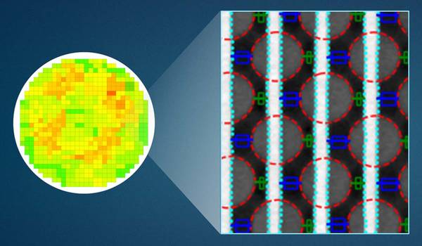
The patterning challenges of today’s most advanced logic and memory chips can be solved with a new playbook that takes the industry from optical target-based approximation to actual, on-device measurements; limited statistical sampling to massive, across-wafer sampling; and single-layer patterning control to integrative multi-layer control. Applied’s new PROVision® 3E system is designed to enable this new playbook.

Breakthrough in Metrology Needed for Patterning Advanced Logic and Memory Chips
As the semiconductor industry increasingly moves from simple 2D chip designs to complex 3D designs based on multipatterning and EUV, patterning control has reached an inflection point. The optical overlay tools and techniques the semiconductor industry traditionally used to reduce errors are simply not precise enough for today’s leading-edge logic and memory chips.
