Products & Technologies
Products & Technologies
Services
Resources
Posted
May 29, 2018

Stay updated on our content.
Further Industry Thoughts on Full-Nodes, Inter-Nodes, Leading-Nodes and Trailing-Nodes – Part 2

May 29, 2018
In part one of this blog, I reported on the 2018 Industry Strategy Symposium (ISS) where Dan Hutcheson of VLSI Research led a panel with representatives of Synopsys, NVIDIA, Intel, ASML and Applied Materials. The participants discussed how the industry is focused on simultaneously squeezing more capabilities from leading-nodes, inter-nodes and trailing-nodes to drive advances in computing. I touched on the use of new materials and 3D techniques to achieve improvements in device performance, power and area/cost – which chip designers call “PPAC.” I explained that in NAND, classic Moore’s Law scaling (more transistors per mm2) hit physical limits, yet the NAND roadmap continued thanks to a transition to 3D architectures (more transistors per mm3). I said that 3D techniques are also being applied in emerging memories (Intel® 3D XPoint™ technology) and even in logic (3D FinFET).
In this blog, I’ll take a slight detour to provide industry context before explaining an important new 3D self-alignment technique called “multicolor,” which Applied’s Prabu Raja alluded to during ISS.
Why This is Critically Important
Our industry faces a paradox: the Internet of Things (IoT) gives us more data than ever before, and big data and AI allow us to process this data in new ways to find valuable, hidden patterns. The data explosion and AI are just beginning to transform major industries, from advertising to agriculture, retailing, transportation, manufacturing, life sciences and healthcare.
At exactly the wrong time, Moore’s Law is slowing: the engine that fueled the previous eras of computing is no longer firing on all three cylinders to deliver needed improvements in performance, power and area/cost. Data is growing faster than transistors are shrinking. And when it comes to performance and power, shrinking is no longer helping the way it used to. Fortunately, new materials, materials engineering and 3D design techniques are extending the roadmap. The industry has an opportunity to collaborate at all levels to speed the development of new materials and design techniques that can enable the promise of AI even as classic 2D scaling reaches physical and economic limits.
A Success Story in Memory
In NAND, we hit the limits of Moore’s Law as the memory cells became so small that we no longer had a sufficient number of electrons to reliably read, write and retain data. However, engineers are clever and they devised new materials (like patterning films) and materials engineering techniques (like staircase etching) to re-arrange the cells to be larger – but also stacked, in skyscraper fashion, so that “A/C” could be continued.
An Emerging Story in Logic
Today, similar thinking is helping to advance the roadmap in logic. Consider 3D FinFET. Surrounding the gate on three sides not only improves performance and power: it also bends the surface area required for the gate skyward, using the Z dimension to allow more individual transistors to be squeezed into the X/Y plane. This is one good example of 3D design techniques coming to logic. Another is Intel’s “contact over active gate” innovation, whereby the contact of the transistor is relocated – from the side of the gate to on top of the gate. The transistor has effectively been reorganized such that parts of it arrive on a second layer that needs to be precisely aligned over the first. Moore’s Law slows, but performance, power and area/cost continue through the clever use of 3D techniques.
Advanced Lithography: Important but not Sufficient
As we learned at ISS, while it is becoming more difficult and expensive, the industry will continue to shrink logic features in 2D. As rising lithography cost is offset with 3D techniques, the most important problem to solve is the vertical alignment of features between one critical layer and the next. We need very precise arrangement of the contacts and vias. As the ISS panelists explained, improvements in 2D scanners can’t fully solve the alignment challenges of a 3D world. We now need materials-based self-alignment techniques.
3D Self-Alignment with Materials Engineering
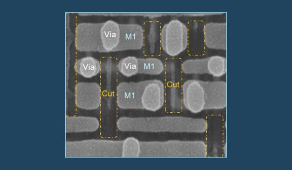
One example of 3D self-alignment is a technique that designers call “multicolor.” Materials engineering can be used to modify the properties of the interlayer used to form the vias connecting two layers. The interlayer can be precisely and iteratively etched and filled to produce an alternating pattern of materials, some that are etch selective and others that are etch resistant. In this way, even when there is significant alignment error in the lithography step used to form the via connecting the upper layer to the lower layer, the etch will only remove the selective material, leaving the non-selective material intact. As a result, the hole that forms the shape of the via is created directly on top of the critical feature, and the via lands exactly where it is intended to be; overlay issues are mitigated as the materials ensure self-alignment.
In short: advanced lithography is made practical by materials engineering. The third dimension is exploited for greater density; contact alignment is improved for better electrical performance and yield; and the process window is relaxed for easier manufacturing. The benefits associated with classic Moore’s Law scaling are extended as 2D scaling is supplemented by new, selective materials and new, selective 3D materials engineering techniques.
The radical new use of materials and materials engineering 3D techniques requires changes in process equipment strategy. Stay tuned for details in Part 3 of the blog, where I’ll explain the transition from unit process systems to integrated systems, and to something entirely new called “integrated materials systems.”
Intel and 3D XPoint are trademarks of Intel Corporation or its subsidiaries in the U.S. and/or other countries.
Tags: nodes, inter-nodes, leading-nodes, trailing-nodes, ISS, full-nodes, AI, artificial intelligence, materials innovation, iot, materials engineering, 3D NAND, vertical scaling, contact over active gate, materials systems
Sundeep Bajikar
Corporate Vice President, Corporate Strategy and Marketing

Sundeep is Head of Corporate Strategy and Marketing (CSM) and guides the executive leadership team in the development of the company's growth thesis, strategic priorities, key initiatives and investor communications. He is also responsible for developing Applied’s marketing capabilities and community. Sundeep’s work served as the foundation for Applied’s strategies related to AI, ICAPS, Heterogenous Integration and Net Zero.
He joined Applied in 2017 after spending ten years as a Senior Equity Research Analyst covering global technology stocks, including Apple and Samsung Electronics, for Morgan Stanley and Jefferies. Previously he worked for a decade as a researcher, ASIC design engineer, system architect and strategic planning manager at Intel Corporation.
Sundeep holds an MBA in finance from The Wharton School and M.S. degrees in electrical engineering and mechanical engineering from the University of Minnesota. He holds 13 U.S. and international patents with more than 30 additional patents pending. Sundeep is also author of a book titled, “Equity Research for the Technology Investor – Value Investing in Technology Stocks.” He was an Institutional Investor Rising Star.

Adding Sustainability to the Definition of Fab Performance
To enable a more sustainable semiconductor industry, new fabs must be designed to maximize output while reducing energy consumption and emissions. In this blog post, I examine Applied Materials’ efforts to drive fab sustainability through the process equipment we develop for chipmakers. It all starts with an evolution in the mindset of how these systems are designed.

Innovations in eBeam Metrology Enable a New Playbook for Patterning Control
The patterning challenges of today’s most advanced logic and memory chips can be solved with a new playbook that takes the industry from optical target-based approximation to actual, on-device measurements; limited statistical sampling to massive, across-wafer sampling; and single-layer patterning control to integrative multi-layer control. Applied’s new PROVision® 3E system is designed to enable this new playbook.

Breakthrough in Metrology Needed for Patterning Advanced Logic and Memory Chips
As the semiconductor industry increasingly moves from simple 2D chip designs to complex 3D designs based on multipatterning and EUV, patterning control has reached an inflection point. The optical overlay tools and techniques the semiconductor industry traditionally used to reduce errors are simply not precise enough for today’s leading-edge logic and memory chips.
