Products & Technologies
Products & Services
Contact
Products & Services
Products & Technologies
Services
Resources
Contact
Posted
July 19, 2018

Stay updated on our content.
Enabling the AI Era with a New Integrated Materials Solution
July 19, 2018
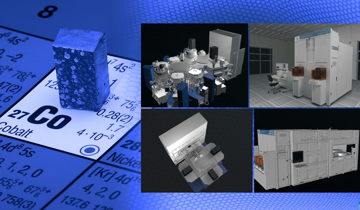
As we enter the foundry 7nm and below technology nodes, tungsten fill for contacts has reached the physical limits of scaling and copper used in the lowest level interconnects is facing challenges on multiple fronts. To address these issues, Applied Materials introduced an Integrated Materials Solution for cobalt to enable the use of a new conducting material. This transition can enable continued device scaling and less power consumption per computation.
Following on my previous blog about the cobalt inflection in chips, I will now discuss the solutions that enable this change—the most significant conducting material change since copper dual damascene was introduced 20 years ago.
Materials Bottleneck
The contact and lower interconnects are the smallest and most critical wiring layers delivering current to transistors, and due to continued geometric scaling of logic semiconductors, these metal layers now create a bottleneck to transistor performance. Both tungsten (contact) and copper (lower interconnects) require liners, barriers and adhesion layers that make extending these materials to 7nm and beyond challenging due to the total thickness of these stack films. For the tungsten contact, the issues include:
- The CVD titanium nitride barrier layer and ALD tungsten nucleation limit cannot be made thinner due to physical limitations.
- Inherent to the CVD tungsten fill is a seam that exacerbates electron scattering, which can lead to performance variation within a device or from die to die.
Cobalt contact metallization, as explained in my previous blog, can use a thinner barrier layer and does not require a nucleation layer, allowing for continued dimensional scaling of the contact. In the case of tungsten, without scaling the liner and barrier layers, there would no longer be pure metal in the contact by the 5nm node. But, if we look at a cobalt contact at 5nm, the volume for cobalt is still 6nm for a similar size contact to tungsten, providing more fill material. And, because cobalt is a lower resistance material than tungsten, the overall resistance of the contact is greatly improved. Also, the seam can be removed from cobalt using an anneal process, further reducing resistance and variance.
Adopting cobalt in the copper interconnect also enables scaling the total liner and barrier thickness, leading to a higher volume of metal. In contrast to the contact, copper has a better bulk resistivity than cobalt, but copper resistance suffers in very narrow lines due to the electron mean free path effect. Finally, the electromigration property of cobalt is significantly better than copper, which improves device reliability.
Integrated Materials Solution for Cobalt
Applied’s end-to-end solution for cobalt interconnects includes deposition, anneal and planarization technologies on our Endura®, Producer® and Reflexion® platforms, respectively. These systems are highly optimized to work together. The Endura platform is used for multiple deposition steps and is the only platform that offers an integrated PVD and CVD cobalt solution. The Producer anneal system provides a truly unique, very high productivity metal anneal chamber for cobalt. The Reflexion LK Prime CMP system removes the overburden material with advanced process control. In addition, the PROVision™ platform provides a new non-destructive electron beam method for cobalt void detection.
Below is the integrated process flow as shown in Figure 1:
- PVD titanium and ALD titanium nitride for the silicide and barrier layers
- PVD cobalt serves as an anchor layer to ensure good cobalt adhesion to the bottom of the feature
- CVD cobalt is then used to deposit a conformal film to bulk fill the feature
- Anneal purifies and reflows the cobalt, removes the CVD seam, and merges crystal grains to form a more crystalline, lower resistance material
- PVD cobalt for a thick overburden film
- CMP removes overburden materials to create a smooth planar surface
- E-beam technology monitors the process and detects voids
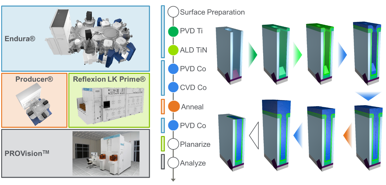
Figure 1: The Integrated Materials Solution for cobalt utilizes four of Applied’s platforms
The integrated process flow for cobalt interconnects was developed at our Maydan Technology Center and the TEM in Figure 2 shows the cobalt gapfill result. One of the benefits from this flow is that even if the feature is re-entrant, which means the top of the feature is narrower than the bottom, the cobalt can still fill this feature without seams or voids.
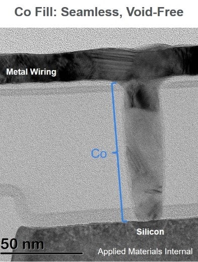
Figure 2. Cobalt gapfill with no seam
The platforms that form our Integrated Materials Solution for cobalt have been industry workhorses for several decades, and the innovations being developed show that they remain critical for the dimensional and materials scaling necessary for the industry to continue improving the power, performance and area/cost (PPAC) of chips.
In summary, cobalt contacts and interconnects can enable continued device scaling to 7nm and beyond. Low-resistance cobalt in narrow features delivers superior device performance and improved power utilization. Applied’s end-to-end solution highlights our leading capabilities in materials engineering and illustrates how we are helping to solve some of the most difficult problems our industry faces.
Tags: Cobalt, interconnects, Moore’s Law, Semiconductors, Integrated Materials Solution, PPAC, materials engineering

Jonathan Bakke
Now is the Time for Flat Optics
For many centuries, optical technologies have utilized the same principles and components to bend and manipulate light. Now, another strategy to control light—metasurface optics or flat optics—is moving out of academic labs and heading toward commercial viability.
Seeing a Bright Future for Flat Optics
We are at the beginning of a new technological era for the field of optics. To accelerate the commercialization of Flat Optics, a larger collaborative effort is needed to scale the technology and deliver its full benefits to a wide range of applications.
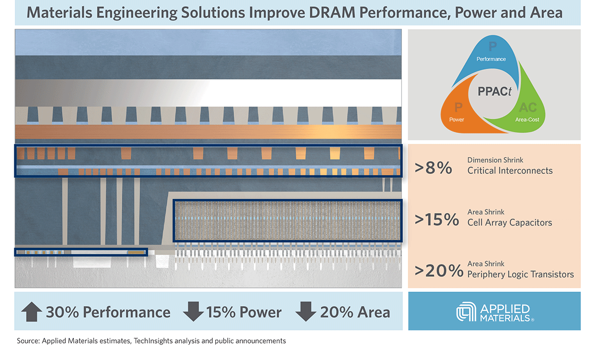
Introducing Breakthroughs in Materials Engineering for DRAM Scaling
To help the industry meet global demand for more affordable, high-performance memory, Applied Materials today introduced solutions that support three levers of DRAM scaling.