Products & Technologies
Products & Technologies
Services
Resources
Posted
June 12, 2018

Stay updated on our content.
Enabling the AI Era with New Materials
June 12, 2018
We are on the cusp of the biggest computing wave yet — the AI era driven by Big Data. Enabling this era will require significant enhancements in processor performance and in the capacity and latency of memory. These requirements are coming at a time when the industry is being increasingly challenged by a slowdown in classic Moore’s Law scaling. What’s needed to continue driving the industry forward are new material combinations systematically engineered at the atomic scale to enable AI with novel architectures and devices.
In this two-part blog series, I will first look at a materials inflection in the transistor contact and local interconnects, followed by a discussion on the need for Integrated Materials Solutions.
The PC era was characterized by classic Moore’s Law shrinking that relied on a small number of materials and on geometric scaling enabled by lithography to improve chip performance, power, area and cost, commonly referred to as PPAC.
By the Mobile era, we saw the original set of materials used in classic Moore’s Law hitting physical limits, and a few new materials were adopted along with changes in device architectures, such as the move from planar transistors to FinFETs, to drive PPAC scaling.
For the AI era, PPAC improvements require many more new and exotic materials. Further, as dimensions shrink, interfaces become an increasingly larger portion of the material in features, and engineering of materials at the atomic scale is a key requirement and challenge.
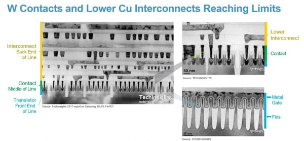
A critical area where new materials are needed is in the contact and local interconnects, which are the smallest level metal interconnects that connect the transistors to the outside world, and are currently fabricated using tungsten and copper, respectively (Figure 1).
New Materials
Applied Materials’ innovative materials engineering work has resulted in the development of a suite of products for the fabrication of transistor contacts and interconnects using cobalt as the conductor. This is the first change in the metal wiring used to power transistors in over 20 years. The last change was the adoption of copper in 1997.
While we will continue to see new architectures and advances in lithography, the most dramatic changes in chipmaking will be in the materials space. From a small number of materials used in the 90s, we expect to see a 10x increase in the number of new materials needed to deliver performance gains to drive wide adoption of AI applications.
Why Cobalt?
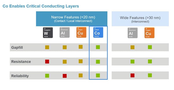
At the 10nm node, using tungsten as a transistor contact metal is a bottleneck to performance due to resistance and gapfill. Similarly, local interconnects fabricated with copper at the M0 and M1 level are suffering in terms of gapfill, resistance and reliability — limiting performance and impacting the cost of manufacturing chips. Replacing the tungsten contact and copper local interconnects with cobalt at the 7nm foundry node and below relieves these performance bottlenecks (Figure 2).
So, what are the benefits of cobalt? Compared to tungsten, cobalt offers inherently superior resistance at small dimensions given its ability to fill small features with a much thinner barrier.
Fabricating tungsten contacts requires a rather thick sleeve with a two-material stack of a barrier and a nucleation layer. The thicknesses of these films cannot be reduced any further as features shrink, limiting the available volume for a conducting metal. As the transistor contact shrinks to ~12nm, it reaches the physical limit where no volume is available for tungsten. A thinner liner barrier can be used with cobalt and at a critical dimension (CD) of 15nm — roughly equivalent to the 7nm node — a 3.7x increase in conducting metal can be achieved.
Adopting cobalt transistor contacts results in a significant reduction in resistance and variability. Based on internal R&D, cobalt contacts are 87 percent less resistive, and variability is reduced from over 10 ohms (normalized) to about 0.06 ohms. These improvements allow more of the inherent performance of the transistor to be realized with less power loss due to lower resistance and with less yield loss due to transistor contact variability reduction.
Even after the transistor contact bottleneck is relieved, the next performance bottleneck is the copper local interconnect. While copper as a bulk metal has a lower resistance than cobalt, there is a crossover point in the 10–15nm range where cobalt interconnects have lower resistance than copper. The cause of this crossover is the electron mean free path — which is ~39nm for copper and ~10nm for cobalt. The electron mean free path defines the length that an electron travels in a bulk material without scattering. When features are below the mean free path, significant scattering occurs at material interfaces and grain boundaries, causing increased resistance. A smaller electron mean free path allows electrons to flow through the narrow line with fewer collisions, resulting in a lower resistance to current.
Also, as mentioned earlier, cobalt works with thinner barriers than copper and as a result, the vertical resistance in the via is lower for cobalt interconnects. For these reasons, cobalt helps unlock the full potential of transistors at the 7nm foundry node and below.
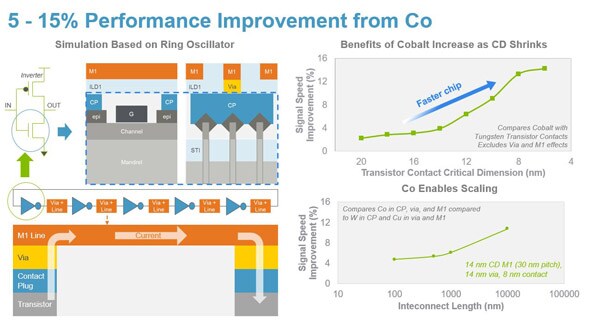
Finally, we have demonstrated the value of cobalt using EDA simulations of a 5-stage ring oscillator circuit. We showed that for a range of CDs simulated, the performance of the circuit with cobalt was better than for tungsten. In fact, this benefit for cobalt increases as CDs shrink, with a highly significant improvement of up to 15 percent in chip performance.
To learn more about the benefits of cobalt and how Applied is enabling its use in the transistor contact and interconnect, I encourage you to watch a replay of our recent webcast or read the transcript, both of which are available here.
Integrated Materials Solutions
Driving classic Moore’s Law in the PC era typically relied on single process system solutions, with fewer integrated processes. In the Mobile era, we saw the development of Integrated Process Systems, to enable the implementation of new materials. Unlike earlier eras, this is not simply the introduction of one enabling material replacing another. Instead it requires multiple innovations, developed in unison across a suite of process technologies that together solve the many challenges required to integrate new materials. The cobalt breakthrough has been enabled by an Integrated Materials Solution approach to address the limitations of tungsten and copper. I will discuss the Integrated Materials Solution for cobalt in more detail in my next blog.
Conclusion
Increasingly we will see PPAC challenges with scaling that need to be addressed with new materials and Integrated Materials Solutions. At Applied, we have the industry’s largest set of materials engineering capabilities available under one roof to explore, develop and integrate — enabling industry inflections. We are uniquely positioned to solve problems with new materials and bring these Integrated Materials Solutions to market to solve the challenges of the AI Era.
Tags: Cobalt, transistor, Moore's Law, artificial intelligence, AI, Integrated Materials Solutions, materials engineering

Jonathan Bakke

Now is the Time for Flat Optics
For many centuries, optical technologies have utilized the same principles and components to bend and manipulate light. Now, another strategy to control light—metasurface optics or flat optics—is moving out of academic labs and heading toward commercial viability.
Seeing a Bright Future for Flat Optics
We are at the beginning of a new technological era for the field of optics. To accelerate the commercialization of Flat Optics, a larger collaborative effort is needed to scale the technology and deliver its full benefits to a wide range of applications.
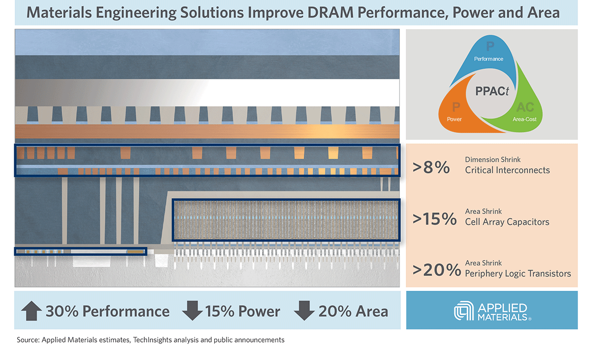
Introducing Breakthroughs in Materials Engineering for DRAM Scaling
To help the industry meet global demand for more affordable, high-performance memory, Applied Materials today introduced solutions that support three levers of DRAM scaling.
