Products & Technologies
Products & Services
Contact
Products & Services
Products & Technologies
Services
Resources
Contact
Posted
December 21, 2023

Stay updated on our content.
Charting a Course Through the Next Era of Technology Inflections: Applied Materials’ Panel During IEDM 2023
by Bala Haran
December 21, 2023
The annual IEEE International Electron Devices Meeting (IEDM) offers a perfect platform to gather thought leaders and make predictions about the direction of the semiconductor industry. For more than a decade, Applied Materials has been using this venue to bring together technologists to discuss and debate the inflections that will drive the leading-edge logic roadmap. Our last discussion in 2019 – “EUV Is Here, Now What?” – heralded the transformative power of AI, Big Data and IoT edge computing to drive profound changes in chip design and manufacturing.
In what turns out to have been a remarkably prescient discussion, the panel concluded that EUV lithography would be a device-scaling accelerant, but that it could not single-handedly address critical chipmaking challenges in the AI era, such as transistor performance and interconnect resistance. Those hurdles, the panelists suggested, would be better addressed through the introduction of new materials, advanced memory and logic transistor architectures, novel interconnect designs, breakthroughs in deposition and etch, and heterogeneous chiplet integration.
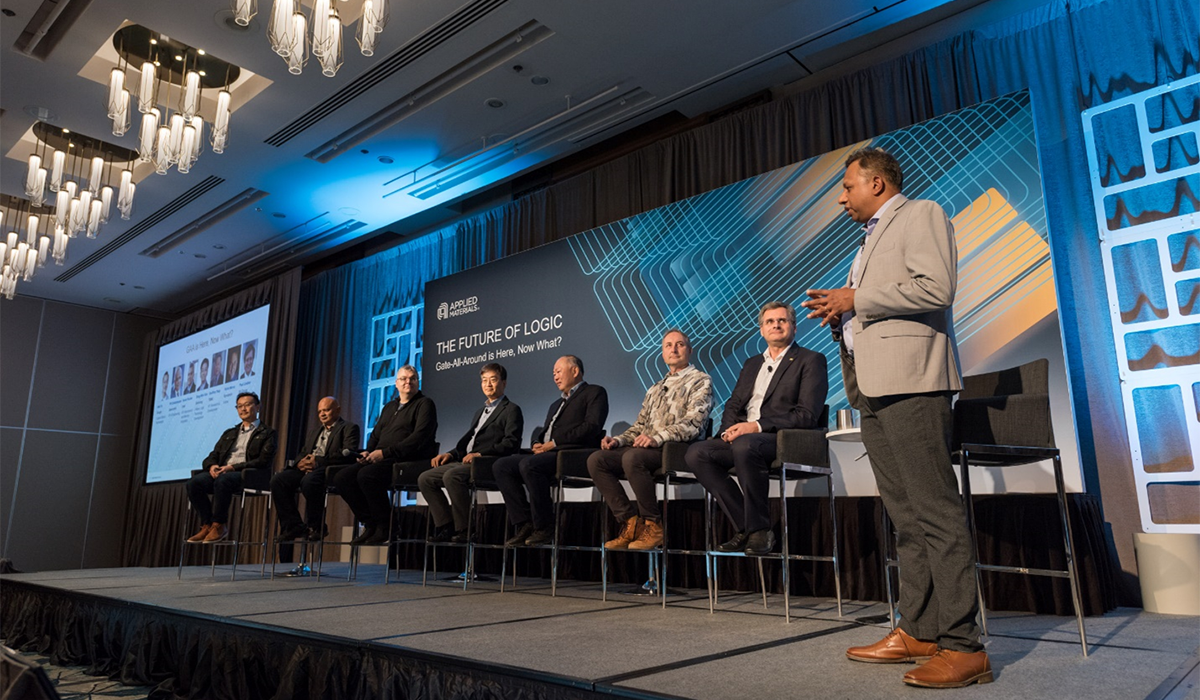
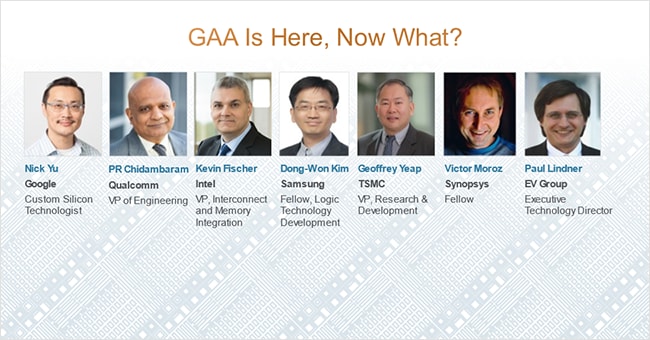
I was thrilled to return to the stage during the 2023 IEDM conference to moderate a panel with a new twist on the same theme: “Gate All Around Is Here, Now What?” With leading technologists from Google, Qualcomm, Intel, Samsung, TSMC, Synopsys and EV Group, we revisited some of the challenges and predictions made in 2019. Collectively, we determined that the gate-all-around (GAA) transistor – just like EUV – is a disruptive innovation that will bring tremendous benefits to chip designers and manufacturers. But it won’t be the solution to every challenge.
To that end, the panel delved into the key transistor and wiring inflections that are driving logic roadmaps, including a look at the benefits these technologies will bring to system designers and the manufacturing challenges that must be overcome to enable high-volume production. So, what has happened since our 2019 panel? I put that question to our distinguished experts, who offered perspectives from their unique vantage points.
Below is a brief summary of my key takeaways from the conversation.
Meeting the Compute Needs of ML Data Centers
I asked Nick Yu, an SoC product development engineering leader at Google, to share some of the applications that are driving the need for new chip manufacturing technologies and their unique requirements.
Nick noted that the explosion of large language models such as ChatGPT have fundamentally changed how Google designs, operates and optimizes its hyperscale data centers. In April 2023, Google launched its TPU v4 for machine learning (ML) applications, which achieved a 10X increase in ML performance, at least doubled energy efficiency and reduced carbon dioxide emissions by up to 20X compared to the previous generation. At the end of 2023, Google introduced its Gemini large language model and announced the deployment of the TPU v5, which runs on a ChatGPT-3 model and doubles overall performance while continuing to lower energy use.
“This shows the magnitude of growth in less than a year,” Nick said. “It didn’t take long for people to start plotting the growth rate of these large language models. If you look at it, this is log scale. This is much steeper than Moore’s Law. My question for the panel and the audience is, will GAA – and even the stacked nanosheets trajectory – keep up with this growth that we’re seeing in large language models in just less than a year?”
Nick added that ML data centers are very specialized compared to classic compute data centers. They need more memory, advanced packaging techniques and novel interconnect technologies – all of which requires system-level thinking and greater collaboration with the chipmaking ecosystem.
Compute Power Remains a Challenge for Mobile
I turned next to Chidi Chidambaram, VP of engineering at Qualcomm. Drawing from his point of view as a smartphone chipset designer, I asked Chidi to share his thoughts on how his teams are helping to cost-efficiently reduce compute and memory access power.
Chidi referenced Qualcomm’s implementation of AI in its products and said there will be an even greater impact as AI moves from the cloud closer to the edge of the mobile network. For Chidi, however, the industry is overlooking a key challenge that needs to be addressed to bring AI to the mobile space.
“If you really look at the true power consumption on a handheld device, the compute power is still a big piece of it,” he said. “Ultimately, voltage reduction and leakage reduction in the transistor operation are fundamental to bringing a lot of these exciting things to a handheld device.”
“While we have a lot of innovations in other areas – we can decrease memory access power, we can decrease RF power – but the compute power has become a larger and larger fraction of the total power and we are not doing as much shrink,” Chidi added. “We have to go back to the bread-and-butter of what has kept this industry going for so long, which is really compute power reduction.”
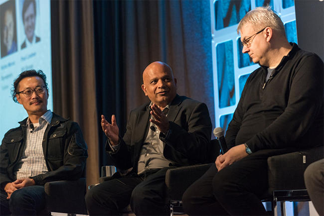
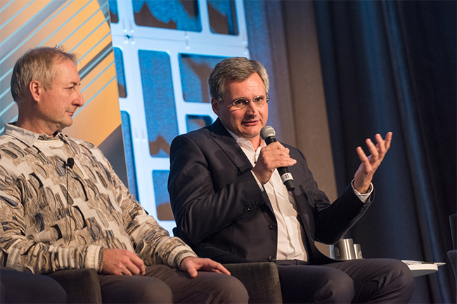
Left to Right: Nick Yu, Google; Chidi Chidambaram, Qualcomm; Kevin Fischer, Intel
Disruptive Innovation is Influencing Logic Roadmaps
I next invited the industry’s leading logic manufacturers, Intel, Samsung and TSMC, to remark on their roadmap strategies. I started with TSMC’s Geoffrey Yeap, VP of R&D and platform development, who is responsible for developing TSMC’s 2nm manufacturing platform, and asked him to explain how his company is managing the complexities of implementing new transistor architectures and power delivery approaches at successive process nodes.
Geoffrey commented that, when he participated on Applied’s EUV-focused panel four years ago, he shared a process roadmap that TSMC is executing successfully today. At that time, the company was just entering 5nm mass production, which has since been followed by 4nm and 3nm, with 2nm on track for volume manufacturing in 2025. He also noted that concerns he expressed at the time relative to interconnect resistance are being addressed through the introduction of backside power delivery, where power is routed to the underside of the wafer – in addition to advances in materials and chiplet packaging.
“The state of logic is strong and the future of logic technology is very bright,” Geoffrey said. “We all know that we need more energy-efficient and high-performance transistors. Nanosheets for the first generation of 2nm are providing a first step in that direction. FinFET has been used – at least by TSMC – for five generations. Hopefully, nanosheets will give us three generations or more.”
Beyond transistor innovations, TSMC is focused on driving 3D integration together with 2D Moore’s Law. By leveraging heterogeneous chiplet integration techniques, TSMC’s customers are building systems with more than 100 billion transistors – and on a trajectory to a trillion transistors by 2030. “We are doing advanced logic plus 3D technology – enabling systems, scaling and integration to deliver the innovative products that offer true leadership in the market,” Geoffrey added. “Four years ago, I introduced to the audience how we develop technology. I think this still stands, but now it's more focused on system performance, not just on the chip or the die performance.”
Intel’s Kevin Fischer, VP and director of interconnect and memory technology integration, leads technology development for the Intel 20A and Intel 18A technologies. Where Intel has historically focused on manufacturing high-performance CPUs for its own internal products, the company is also pursuing a foundry roadmap. Intel was also first to announce a backside power delivery technology it calls PowerVia. How have these developments driven design and technology strategy?
Kevin echoed Geoffrey’s sentiment that the logic roadmap is strong and the pace of innovation remains high. Kevin pointed out that Intel has been vocal about introducing five nodes in four years and is about halfway through that journey. At the same time, logic is becoming progressively more complex, requiring vendors and OEMs to work together to solve the biggest challenges. That is especially true as Intel complements its own high-performance solutions with its foundry program, where it must address multiple customer needs.
“We are focusing not just on high-performance compute, but the needs of mobile and other applications as well,” said Kevin. “I think our roadmap, our innovations and the order in which we bring them is going to be a function of our customers – how the customers react to those technologies, how much benefit they’re seeing. With PowerVia, we see a lot of benefit. It has a lot of value for high-performance compute, but it’s also a way of generating PPAC benefit. It’s hitting all of the vectors.”
Kevin noted that PowerVia not only increases performance and reduces power and cost, but it provides a new level of design flexibility. “It’s giving us better density and it’s not driving some of the key portions of the technology into those very high-complexity zones,” he added. “It enables you to back off pitches a little bit and prevent that escalating cost on your lowest-density layers.”
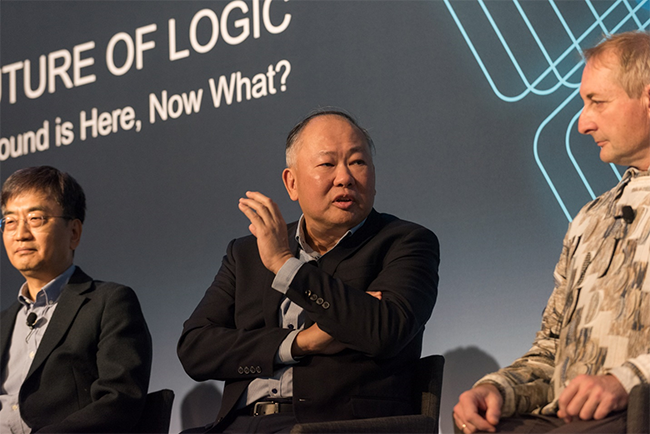
Left to Right: Dong-Won Kim, Samsung; Geoffrey Yeap, TSMC; Victor Moroz, Synopsys
Samsung embraced GAA transistors early on and introduced the technology with its 3nm node. I asked Dong-Won Kim, fellow of Logic Technology Development, to elaborate on that effort. Dong-Won said Samsung foresaw the time when FinFETs would reach their physical height – and performance – limits, which prompted the company to develop GAA as a means to extend transistor performance while reducing power consumption.
Samsung’s first-generation GAA transistor was the GAA MBCFET, also known as the multi-bridge channel field-effect transistor, which it began developing in 2003. Dong-Won cited three primary challenges that Samsung encountered along the way. The first was tightly managing defect inspection and metrology at the GAA structure, which is more difficult compared to FinFET gate structures. The second was to compensate for the limited spacing between vertical nanosheets, and the third was co-optimization of a device with wide nanosheets.
“This is one of the GAA advantages that provides our designers with more design flexibility,” Dong-Won said. “We wanted to do more scaling and we wanted to enhance the performance as well as reduce the power based on the transistor. As Chidi already mentioned, that is fundamental – without that kind of transistor innovation, we couldn’t extend the technology. Samsung really wanted to extend leadership of the technology based on the transistor. That is why we are really focusing more on the GAA MBCFET.”
Dong-Won also highlighted the next transistor inflection point on Samsung’s radar: the transition to stacked nanosheet transistors, also referred to as CFET (complementary field-effect transistors). The main driver behind this technology, he said, is the ability to continue scaling the transistor standard cell.
DTCO and Hybrid Bonding Take the Stage
For perspective from the software and equipment ecosystem, I asked Synopsys and EV Group to share what the industry needs to do to support an increasingly complex foundry roadmap and encourage deeper engagement between design and manufacturing.
Victor Moroz, a Synopsys fellow, said the industry’s commitment to GAA transistors, backside power and 3D stacking is being led by a transition from lithography-driven scaling to design-technology co-optimization (DTCO), which is focused on performance, power efficiency, transistor density and cost.
“Once DTCO becomes the main driver of technology, the turnaround time for DTCO iterations becomes more important,” Victor said. “If it was litho-driven scaling, then you just do your new patterning and you’re in business. With DTCO, you have to evaluate several different scaling boosters and performance boosters to see what works better, what can be done in the right time. We are working on technologies to automate and shrink that time.”
Victor Moroz, Synopsys; Paul Lindner, EV Group
Representing the equipment sector on the panel, EV Group (EVG) weighed in on the significance of wafer-level packaging and the emergence of hybrid bonding. Paul Lindner, executive technology director, observed that NAND flash already uses hybrid bonding, where each NAND wafer is made by combining two separate wafers.
Bonding enables new system architectures, according to Paul, which allows for the integration of new materials – and new ideas. EVG has already shown the scalability of hybrid bonding by working together with Applied Materials to demonstrate a sub-400nm pitch and believes it can achieve a 100nm pitch.
“Complementing the traditional scaling with stacking is the main theme of 3D, and we try to play a major role there,” Paul said. “Our owner and founder came to me once in my early days at EVG and said, ‘It doesn’t make sense to use only the front side of an expensive wafer. There’s an equivalent back side.’ I like to refer to our products as scaling boosters. They allow us to access the back side by enabling TSVs and in the front side by giving access to transistor cells with the backside power delivery networks. And in between, the hybrid bonding of two relatively completed wafers provides performance and scaling. The common theme here is really that bonding enables a new system architecture."
Conclusion: The Twin Engine
In closing the wide-ranging panel, I asked the audience to remember two key takeaways: the future of logic is bright, and AI is going to change the world. Geoffrey Yeap of TSMC drove this point home with an apt analogy: For many years, the mobile revolution was the engine that drove the semiconductor industry. “I hope the AI revolution – driven by semiconductors – will be another engine that we have been looking for,” he said. “Besides mobile, now we have a twin engine, and I hope this aircraft will fly high and far.”
Bala Haran, Ph.D.
Vice President, Integrated Materials Solutions

Dr. Bala Haran is Vice President of Integrated Materials Solutions at Applied Materials where he leads a team of device integrators and process engineers focused on identifying and enabling new inflections in logic and memory technology. Prior to joining Applied, Bala was at IBM for 18 years where he led multi-company process and device integration teams focused on CMOS technology development and transfer. He holds a Ph.D. in chemical engineering from the University of South Carolina and has more than 50 peer-reviewed publications and 100 patents granted.

Revisiting the Future of Logic at IEDM 2023
Applied is showing up in full force at the 2023 IEEE International Electron Devices Meeting (IEDM). In addition to presenting at important conference sessions, Applied will be hosting a thought-provoking panel discussion featuring leading technologists from Google, Qualcomm, Intel, Samsung, TSMC, Synopsys and EV Group.
New Innovations Needed to Continue Scaling Advanced Logic
The semiconductor industry is at a crossroads. Demand for chips has never been greater as we enter the early stages of a new wave of growth fueled by the Internet of Things, Big Data and AI.
_1200x700.jpg)
AI and Big Data Are Disrupting the Semiconductor Industry as We Know It
The recent IEEE International Electron Devices Meeting (IEDM) reaffirmed that the semiconductor industry is in a period of reinvention as we grapple with the challenges and opportunities promised by the Internet of Things (IoT), Big Data and AI.