Products & Technologies
Products & Technologies
Services
Resources
Posted
February 07, 2019

Stay updated on our content.
Applied Materials Collaborates with IBM on AI Chip Technology

by Gary Miner
Feb 07, 2019
One of the most debated topics of conversation at technology conferences recently is how will the semiconductor industry deliver the dramatic improvements in chip performance per watt needed for AI to reach its full potential. While there are many differing opinions on the matter, one thing is clear—it will require disruptive innovation across the technology ecosystem. Relying solely on shrinking transistors won’t do it; we need new chip architectures, new materials and processes, and new integration schemes—in other words, it takes the effort of more than one company.
Applied Materials has been championing the notion that a “New Playbook” for semiconductor design and manufacturing is needed for the AI era, one that speeds connectivity across the ecosystem—from materials to systems. As part of this effort, I am excited to announce Applied’s participation as a member of the new IBM Research AI Hardware Center, also unveiled today by IBM.
The IBM Research AI Hardware Center will provide an environment where research and commercial partners can collaborate with IBM to further accelerate the development of AI-optimized hardware innovations. The Center will host R&D, emulation, prototyping, testing and simulation activities for new AI cores specially designed for training and deploying advanced AI models. As the leader in materials engineering, Applied will provide expertise in researching new materials that can potentially help improve performance, power and cost for next-generation AI chips. We will maintain a strong focus on the application of these new technologies to AI workloads.
The semiconductor industry has overcome many formidable challenges over the decades, and I am confident we can work together to close the gap between what’s achievable today and where we need to be in terms of the performance per watt desired by the AI community. Applied is excited to be among the companies driving this effort with industry leaders like our long-time technology partner, IBM.
Tags: artificial intelligence, AI, IBM, materials engineering, r&d
Gary Miner
Vice President, R&D Alliances

Gary Miner is vice president of R&D alliances at Applied Materials. Gary was previously in charge of strategy and marketing for the Transistor and Interconnect Group. He earned both his master’s and bachelor’s degrees in electrical engineering from Stanford University, and has been with Applied since 1988.

Now is the Time for Flat Optics
For many centuries, optical technologies have utilized the same principles and components to bend and manipulate light. Now, another strategy to control light—metasurface optics or flat optics—is moving out of academic labs and heading toward commercial viability.

Seeing a Bright Future for Flat Optics
We are at the beginning of a new technological era for the field of optics. To accelerate the commercialization of Flat Optics, a larger collaborative effort is needed to scale the technology and deliver its full benefits to a wide range of applications.

Introducing Breakthroughs in Materials Engineering for DRAM Scaling
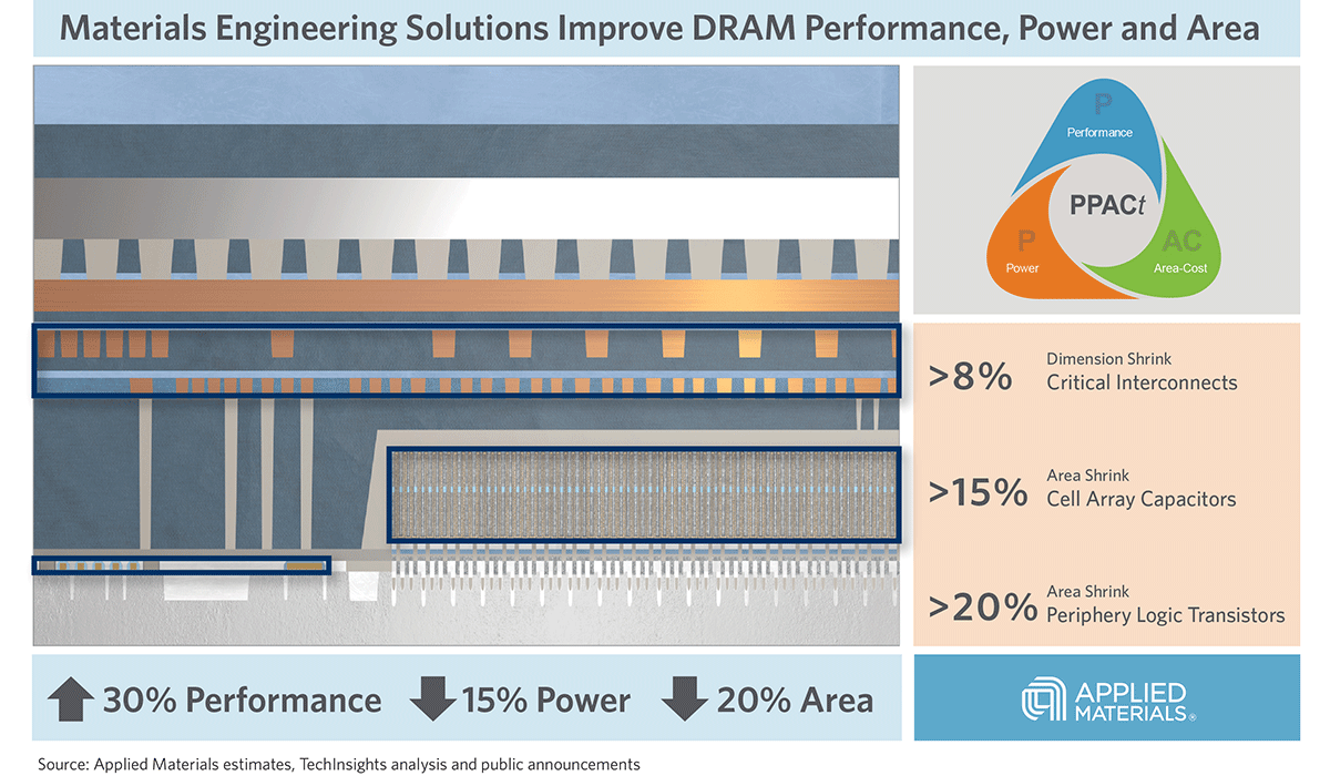
To help the industry meet global demand for more affordable, high-performance memory, Applied Materials today introduced solutions that support three levers of DRAM scaling.
