Products & Technologies
Products & Services
Contact
Products & Services
Products & Technologies
Services
Resources
Contact
Posted
May 30, 2024

Stay updated on our content.
Advanced Logic and Memory Need New Tools for Optical Wafer Inspection
by Ganga Sivaraman
May 30, 2024
Semiconductor production is an expensive and complex endeavor. The journey from R&D to high-volume manufacturing is a race, and whoever crosses the finish line first wins competitive advantage in terms of revenue, market share and profitability. Advanced chips are built up one layer at a time, and each of the billions of individual features must be perfectly patterned and aligned to create working transistors and interconnects with the best performance and power characteristics.
In both advanced logic and memory, the number of processing steps is increasing as we add more and more complexity to the latest and greatest chips. Defects introduced in between the process steps directly impact wafer yields and ultimately slow down an economy that runs on silicon. Patterned wafer inspection – the scientific study of defects across the entire wafer manufacturing lifecycle – has always been critical to controlling and perfecting the chipmaking process. However, as chip structures become ever smaller and the process grows in complexity, the way we inspect leading-edge chips needs to evolve.
More Complexity Calls for More Inspection
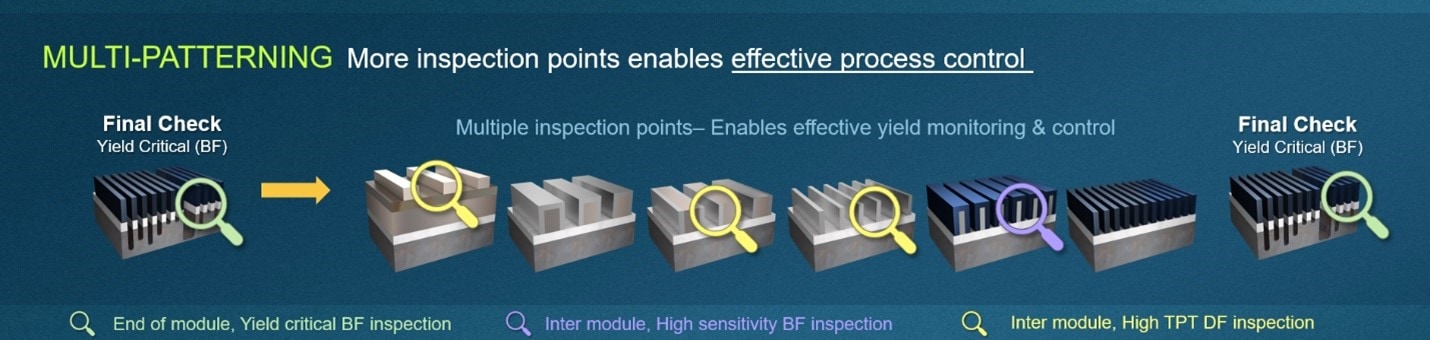
Management guru Peter Drucker is credited as saying, “what gets measured, gets managed.” Often, fab inspection strategies analyze data from a limited number of intermediate and end-of-module steps. But as process complexity increases, and techniques like multipatterning invite minor defects to become magnified, we need to gather data from all key process modules. Otherwise, defects and process drift may not become visible until engineers are faced with costly and inexplicable yield issues.
When determining where and how often to inspect, the right technical answer is, “more is better.” At the same time, fab managers need to control costs, which is why they must deploy an optimized approach that uses the most cost-efficient tools for the job. A mix and match of optical inspection approaches – both brightfield and darkfield – is the key for cost-effective yield monitoring and control.
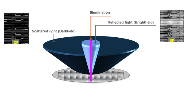
Brightfield and darkfield wafer inspection technologies are complementary and typically used for addressing different application needs. Brightfield primarily collects reflected light, with the source of illumination oriented perpendicular to the wafer’s surface. Light bounces off the surface and returns a “bright” image showing a realistic view of the patterned features on the wafer, similar to the way a mirror shows a clear and precise reflection of a person’s face. With darkfield, the wafer can be imaged using either normal illumination or oblique illumination, where the light is at an angle to the wafer surface. Darkfield focuses primarily on collecting scattered light. When a beam of light encounters angled or rough surface features within a chip’s nanoscale patterns, its trajectory is altered. Collecting this scattered light produces images of the edges of 3D structures against a dark background.
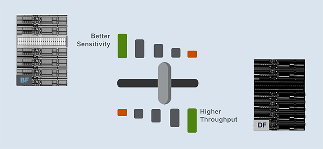
Brightfield inspection primarily targets high-sensitivity applications and delivers lower inspection throughput. Darkfield is suited to lower-sensitivity applications — typically targeting defects of 20nm or greater in size — and delivers very high inspection throughput.
Wafer Inspection at a Crossroads
New challenges in advanced logic and memory are calling for a new playbook for optical wafer inspection. Chipmakers are telling us that they need new capabilities which maintain the high throughput and low cost-of-ownership characteristic of darkfield inspection while delivering optimal sensitivity for both 3D surface defects and surface pattern defects.
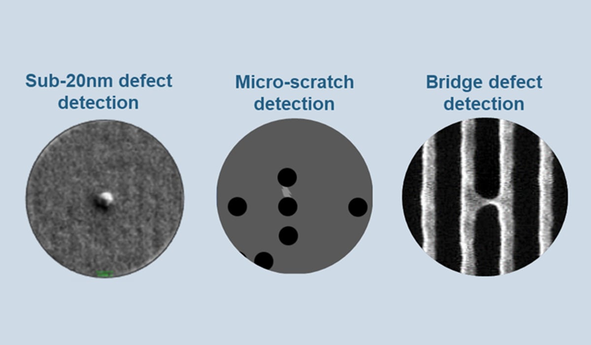
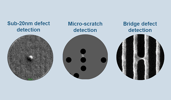
For example, defects in the sub-20nm range have traditionally been considered too small to have a significant impact on wafer yield and therefore have not been a priority for optical inspection. As the critical dimensions of devices continue to shrink, defects in this size range become more problematic. If left undetected, these small particles can block etching and cause pattern defects in subsequent steps. Traditional darkfield tools do not have the resolution to detect these critical defects of interest.
Likewise, when creating the vias that connect vertical layers of metal interconnects, tiny micro-scratches can be left behind in the oxide layer after chemical mechanical planarization (CMP) steps. These scratches must be detected early before they turn into bridge defects when the vias are filled with metal.
Applied Materials has a strong presence in the optical inspection market with its Enlight® wafer inspection system which offers brightfield and darkfield modes. We believe chipmakers who are pushing the leading edge of logic and memory will eventually need a next-generation darkfield tool that can deliver a new combination of darkfield application sensitivity and throughput.
Based on extensive customer engagements, we are preparing to introduce a state-of-the-art wafer inspection system designed to deliver the industry’s highest darkfield application sensitivity at higher throughput. Our solution is designed to make it cost-effective for chipmakers to inspect more inter-module process steps, enabling them to effectively monitor and control wafer yield. With more than 10 customer engagements in 2023, we have successfully demonstrated our capabilities in high-throughput wafer inspection in a variety of processing modules such as deposition, CMP, lithography, etch, implant and a few custom modules. We look forward to sharing more details about the new inspection system in the coming months.
Ganga Sivaraman
Product Marketing Director, Optical Patterned Wafer Inspection

Gangadharan (Ganga) Sivaraman is Product Marketing Director for the Optical Patterned Wafer Inspection division at Applied Materials. Prior to joining Applied, he held various application engineering, marketing and program management roles at KLA. Ganga's experience and expertise spans FEOL/BEOL process control solutions and yield improvement methodologies. He holds a master’s degree in electrical engineering from Texas Tech University.
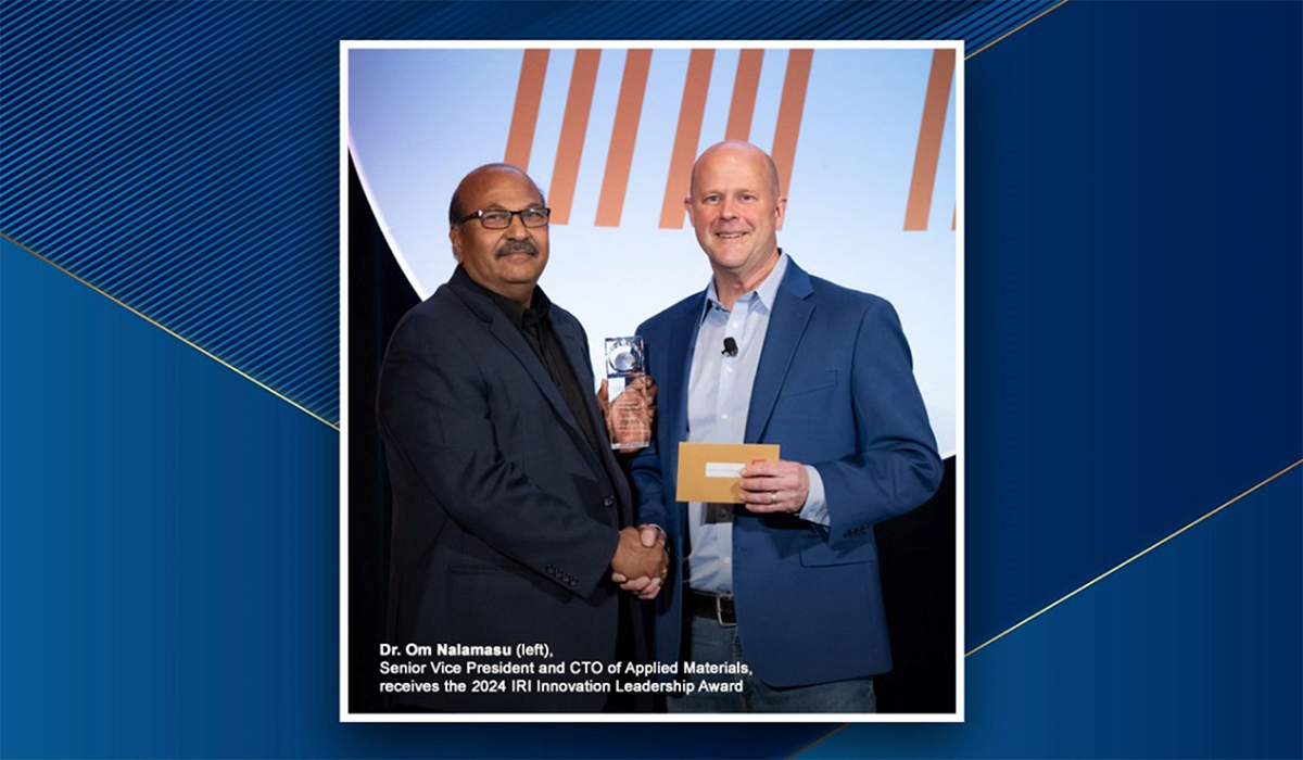
Celebrating Innovation: Dr. Om Nalamasu Receives the 2024 IRI Innovation Leadership Award
As an industry leader, Applied Materials is constantly innovating. Whether it’s breakthroughs in materials engineering or pioneering new ways of working with our customers and partners, being able to innovate quickly and with a high success rate is paramount to our continued leadership and growth.
HBM: Materials Innovation Propels High-Bandwidth Memory Into the AI Era
Nvidia’s CEO Jensen Huang famously referred to the launch of OpenAI’s ChatGPT as an “iPhone moment” for artificial intelligence, describing it as “one of the greatest things that has ever been done for computing.”
Applied Materials Showcases Memory Innovations at IMW 2024
Large language models (LLMs) have been around for years, but they only recently entered the popular lexicon with the launch of ChatGPT and the ensuing generative AI boom.