Products & Technologies
Products & Services
Contact
Products & Services
Products & Technologies
Services
Resources
Contact
Posted
October 30, 2023

Stay updated on our content.
Enlight® 2: Accelerating Brightfield Optical Inspection in a New Era of Chipmaking
by Gilad Reut
October 30, 2023
Yield has long been considered one of the most critical metrics in semiconductor manufacturing. Reducing the time needed to ramp a process to production-level yields can be worth billions of dollars to chipmakers. That’s why manufacturers invest heavily in wafer inspection techniques to help find and correct yield-killing defects quickly, preferably even before they impact fab output.
There are two complementary tools in the defect-detection toolbox: inspection and review. In the most common strategy, chipmakers use optical light-based inspection to detect potential defects on the wafer, followed by eBeam review, which has the much-higher resolution needed to see and characterize defects by type to help engineers discover and address their root causes. Optical defect detection and eBeam defect review are complementary – the former scans wafers in less time at the sacrifice of resolution, while the latter offers high resolution but takes much longer to scan a wafer. The optimal strategy is to combine the best of both tools.
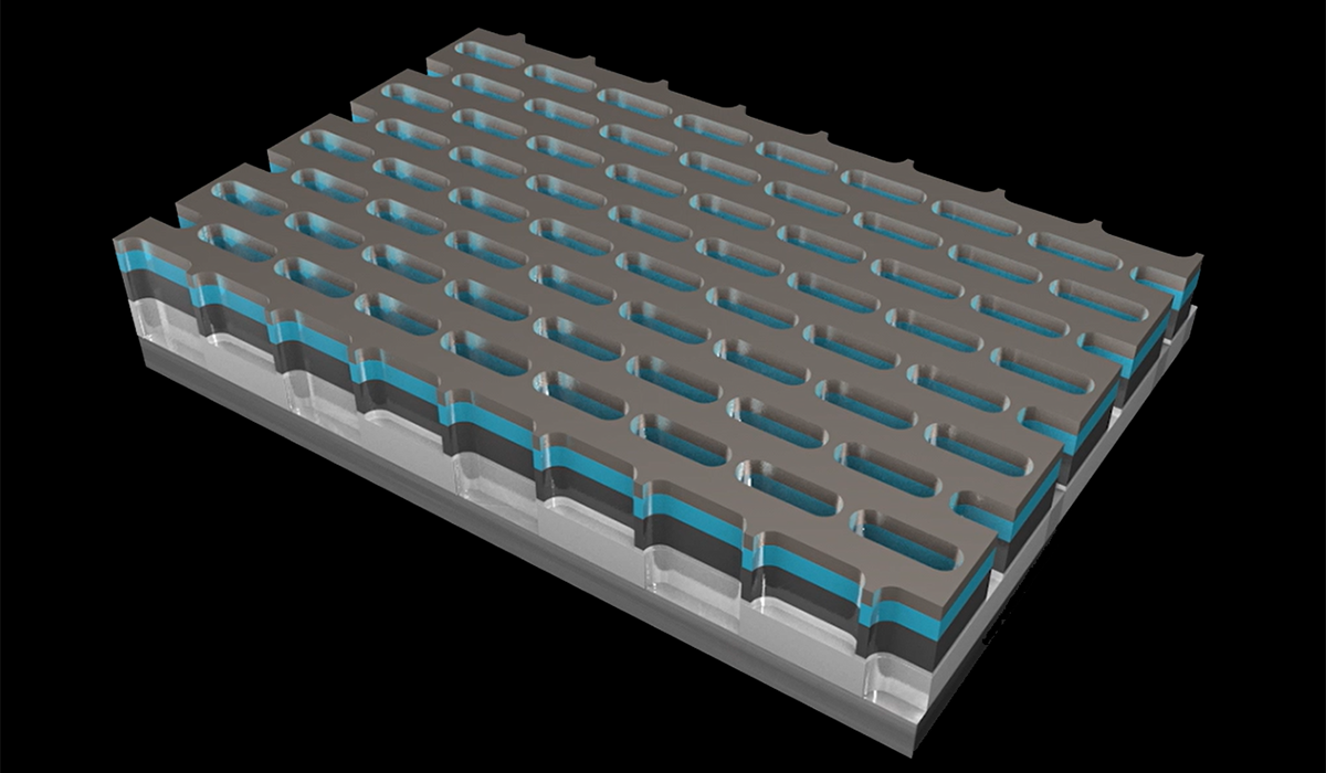
Optical inspection is running up against challenges, however, as semiconductor designs become increasingly complex. As line widths shrink, small nuisance particles become killer defects. As device architectures transition to 3D, particles become harder to detect and see. And as multi-patterning and 3D architectures increase the patterning interdependencies of adjacent process steps, more inspection points are needed to trace defects back to their root causes. Chipmakers increasingly face a cost dilemma: either inspect more and increase manufacturing cost, or save cost and reduce manufacturing yield.
In 2021, Applied launched an innovative optical inspection system designed to help chipmakers navigate this new era of complexity. Our Enlight® brightfield optical wafer inspection system combines industry-leading speed with high-resolution optics that capture more yield-critical data from each wafer scan. It is the only system with simultaneous brightfield and darkfield detection channels – enabling it to collect both reflected light and high angle scattered light to detect the smallest defects.
The Enlight system architecture changed the economics of optical inspection, resulting in a 3X improvement in the cost of capturing critical defects. The cost advantage allows Enlight system customers to reduce inspection budgets or insert more inspection points to detect more particles and patterning errors at the same budget. As a result, the Enlight system has become the fastest-ramping inspection system in Applied’s history, adopted in high-volume production at all of our leading-edge foundry-logic customers.
Today, we are excited to launch the Enlight® 2 system, which brings new levels of throughput and sensitivity.
Distinguishing nuisances from defects
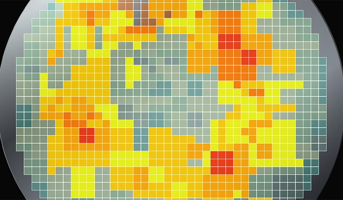
The Enlight 2 system is designed to detect the highest number of yield-killing defects while maintaining low false-alarm rates.
Enlight 2 features two upgrades that increase sensitivity to defects of interest:
- A step function in image processing capabilities and an increase in the imaging dynamic range, together detecting over 100X more potential defects with each scan.
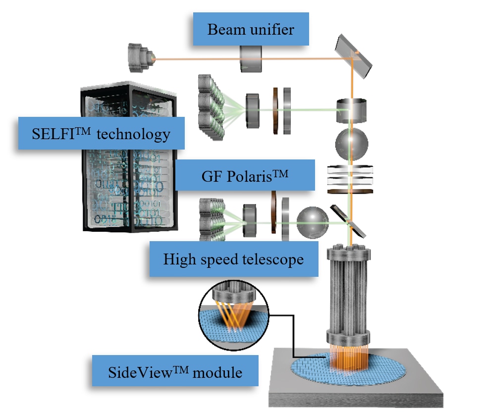
- A new SideView™ module enables oblique illumination of the wafer, which nearly doubles the sensitivity for detecting 3D defects.
The system also offers new capabilities for nuisance suppression:
- A new deep learning engine called SELFI™ detects and classifies more than a billion defect images, enabling engineers to capture 3X more target defects.
- A new light polarization module called GF Polaris™ extends 360-degree tunable polarization to control the greyfield detection channel and reduces nuisances by 50%.
Raising the speed limit
Enlight 2 includes several enhancements that further increase the system’s throughput:
- A new hybrid computing architecture leverages graphics accelerators and dedicated image processors to increase CPU performance by 4X, data storage speed by 5X and networking throughput by 2.5X.
- A new telescope expands the system’s wafer scanning throughput by more than 40%.
Reducing the cost of ownership
These improvements in speed and sensitivity enable chipmakers to insert more inspection points in the overall manufacturing flow while providing more scan sets per recipe, all while maintaining the same overall cost of ownership. At the same time, the increased quantity of actionable information during the inspection stage enhances the ability to predict yield excursions before they occur, immediately detect excursions so that wafer processing can be halted to protect yields, and enable root-cause traceback to accelerate corrective actions and the return to high-volume manufacturing.
Chipmakers tend to lower the sensitivity of inspection tools to minimize nuisance detection, which increases the risk of missing critical defects. To alleviate this challenge, Applied’s ExtractAI™ technology uses big data to help customers rapidly create fully classified, noise-free maps during in-line monitoring. The predictive capabilities of the Enlight 2 system combined with ExtractAI provides a real-time, intelligent link between brightfield optical wafer inspection and our industry-leading eBeam review system, SEMVision®. ExtractAI technology uses artificial intelligence (AI) to characterize all potential defects on a wafer, delivering an actionable map of classified defects to the SEMVision eBeam system. The eBeam system in turn trains the ExtractAI technology to classify yield-killing defects – providing the ability to quickly and accurately distinguish yield-killing defects from the millions of nuisance signals generated by high-end optical scanners. By combining our best-in-class optical inspection and eBeam review technologies, we have created the industry’s only solution with the intelligence to not only detect and classify yield-critical defects but also learn and adapt to process changes in real time.
While the Enlight 2 system is being announced today, we have already shipped a double-digit number of systems to customers for use in high-volume production, demonstrating that we can boost throughput by 50% with no sacrifice in sensitivity. Our goal is to generate over a billion dollars in revenue over the next few years and help our customers generate billions more as they increase fab output and yield in a new era of chipmaking.
Gilad Reut
Product Marketing Expert, Process Diagnostics and Control Group

Gilad Reut is a product marketing expert in the Process Diagnostics and Control group at Applied Materials. He joined Applied in 2014 and is responsible to lead Applied Materials’ Optical Patterned Wafer Inspection Line Monitoring marketing activities. Gilad holds a BSc in Materials engineering from Ben-Gurion University and a MSc in Chemistry from Weizmann Institute of Science.
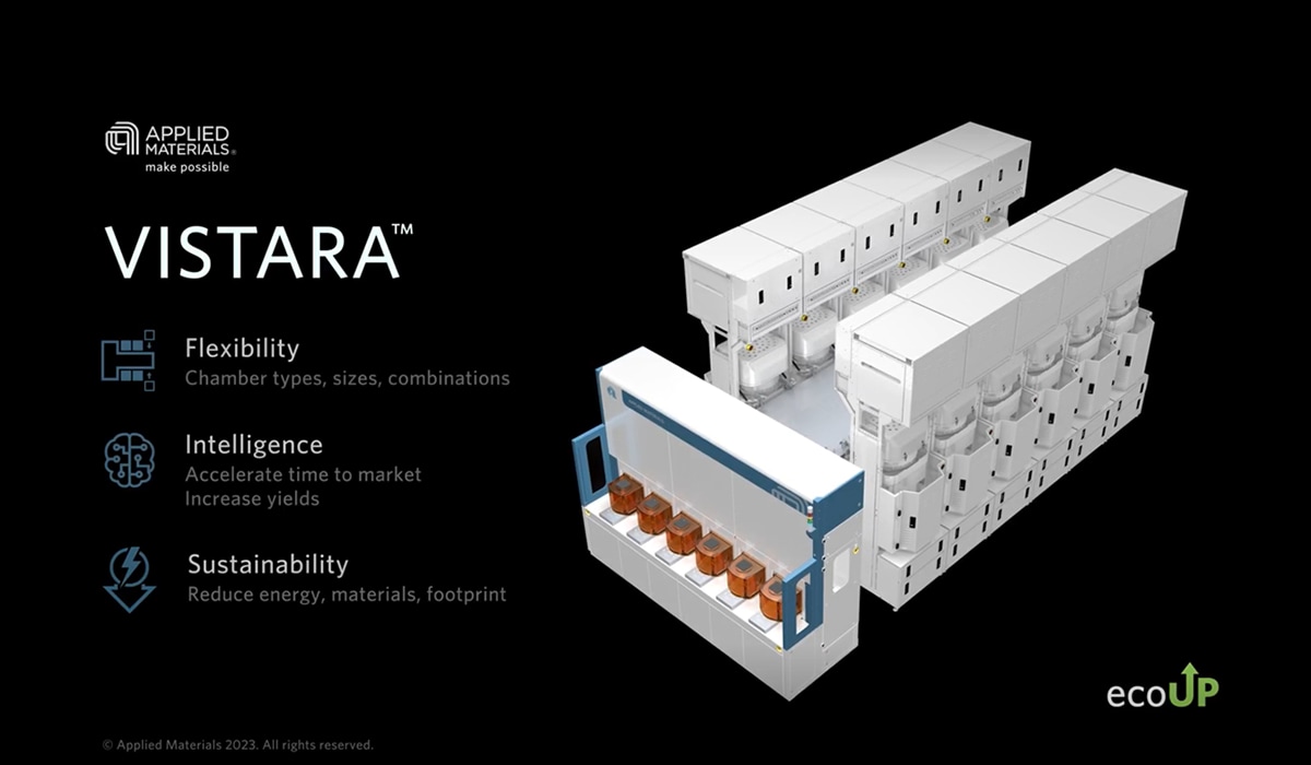
A Deeper Look into the New Vistara™ Platform
Today marks a major milestone in Applied Materials history. At SEMICON West 2023, we introduced Vistara™, a wafer manufacturing platform designed to provide chipmakers with the flexibility, intelligence and sustainability needed to tackle growing chipmaking challenges.
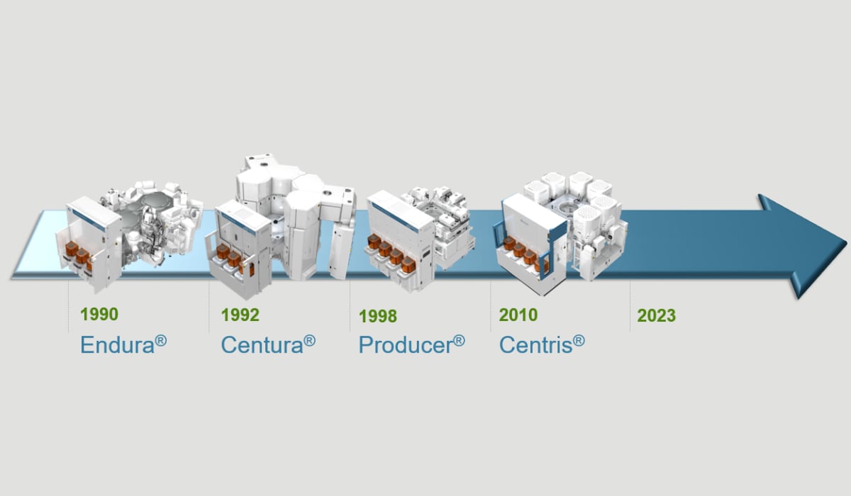
A New Equipment Platform for a New Era of Chipmaking
Most semiconductor industry observers know it takes hundreds of process steps to make a chip. They can picture overhead transfer systems speeding orange FOUPs (Front Opening Universal Pods) full of wafers from tool to tool, imagining each process step being executed as quickly as physics allows before the wafers are zipped off to the next machine. They can sense the science behind the high-stakes race to produce the most precisely completed wafers in the shortest possible time.
Bringing the Future of Advanced Patterning into Focus at SPIE
This year’s SPIE Advanced Lithography + Patterning conference comes at a time when the semiconductor industry needs new breakthroughs to solve the patterning challenges of continued scaling with EUV lithography which will become more intense with the arrival of High-NA EUV.