Products & Technologies
Products & Services
Contact
Back to Menu
Products & Services
Products & Technologies
Services
Resources
Contact
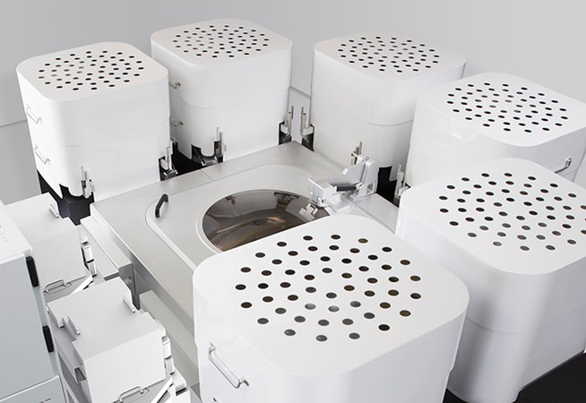
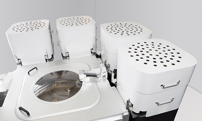
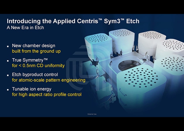
Centris® Sym3® Etch
As semiconductor scaling has continued, increasingly rigorous requirements for precision and uniformity in chip fabrication have propelled the first comprehensive redesign of the silicon etch chamber in over a decade. The resulting Applied Centris Sym3 system delivers world-class cross-wafer uniformity with unprecedented within-chip feature control in critical etch applications for high-volume manufacturing at the 1x/10nm node and beyond.
At earlier technology nodes, when features were larger, a greater range in variation in etch depth, line or space width, or profile angle could be accommodated without affecting device performance. Similarly, occasional particles remaining on feature surfaces did not jeopardize device reliability. At the 1x/10nm node, however, the slightest differences in etch depth, line or space width, or profile angle can be fatal flaws in chip manufacture. And defect-free surfaces are equally essential.
To achieve the tight degree of within-chip etch control needed for such precise patterning, the new system creates a dramatically cleaner chamber environment that significantly accelerates the removal of etch byproducts—a major cause of variation. Both larger chamber volume and higher gas flows minimize the amount of byproduct that redeposits on the wafer, where it can pinch off narrow spaces and create etch depth variations, cause unacceptable variations between densely packed and isolated features, or exacerbate line edge roughness. Preventing byproduct accumulation also reduces particle formation and resultant defect creation.
Etch byproducts build up on feature sidewalls, pinching off
narrow openings. Narrow features therefore cannot be etched
as deeply as wider ones, an effect known as depth loading.
Etch byproducts accumulate more on the sidewalls of isolated
features than on those of densely packed features. Consequently
their final widths differ, an effect known as pattern loading.
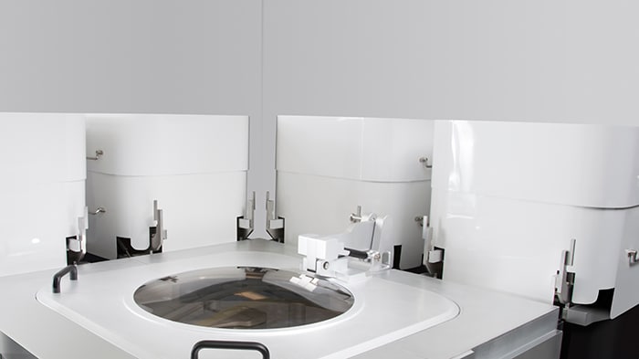
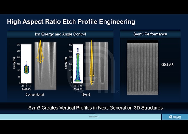
Ensuring that this enhanced within-chip etch precision extends across the entire wafer, the Centris Sym3 system has been comprehensively redesigned for True Symmetry™ of power, gas delivery, and thermal characteristics necessary. In addition, improvements to Pulsync™ increase the effectiveness of synchronized plasma pulsing to minimize pattern loading. Users can enhance further performance with optional dual frequency bias that facilitates the etching of challenging high aspect ratio features.
The redesigned Sym3 chamber environment makes possible process control to within a few atomic layers within chip, chip to chip, and wafer to wafer. The Centris platform delivers the excellent repeatability and high productivity demanded for high-volume manufacturing through system intelligence software that ensures exact process matching among the six etch chambers and between the two plasma clean chambers mounted on the platform.
- 1 / 5
- 2 / 5
- 3 / 5
- 4 / 5
- 5 / 5