PROVision 10 전자빔 계측
반도체 기능은 계속 확장되고 디바이스 아키텍처는 더욱 정밀하고 복잡해지면서, 제조 공정은 더 많은 단계와 엄격한 공정 제어를 요구합니다. 최첨단 칩 설계는 기존의 광학 기반 추정, 통계적 샘플링, 단일 레이어 제어를 뛰어넘는 새로운 계측 기술을 필요로 합니다.
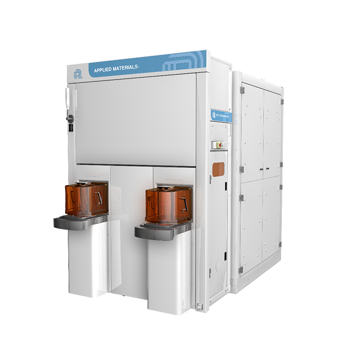
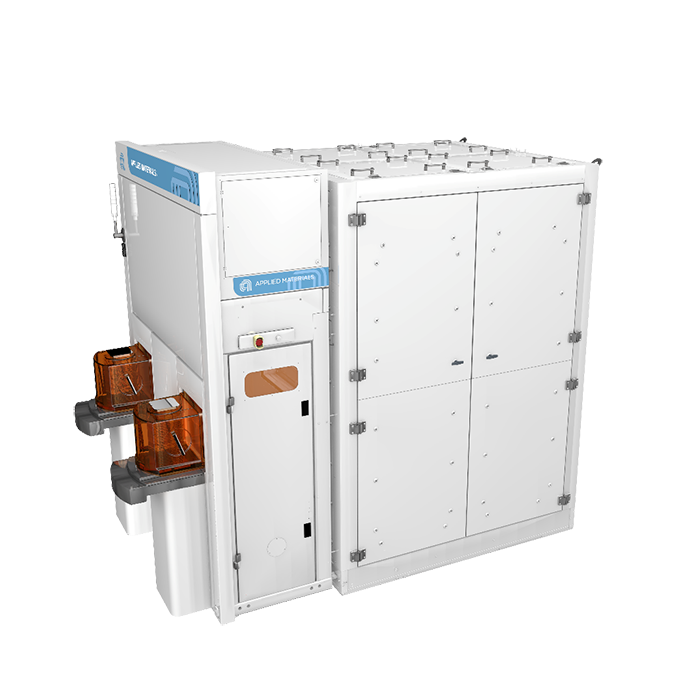
PROVision™10 시스템은 서브 나노미터의 해상도, 고속 처리, 레이어 관통 이미징, 첨단 알고리즘을 결합하여, 2nm 파운드리 로직 칩, GAA 트랜지스터, 차세대 DRAM 및 HBM 메모리, 후면 전력 공급 등 첨단 설계를 정밀하게 패터닝하는 데 필요한 수백만 개의 데이터 포인트를 생성합니다. 이러한 기능을 통해 광학 계측의 한계를 넘어 웨이퍼 전체와 칩의 다층 구조에서 정밀한 측정을 통해 최고의 칩 성능을 달성하고 시장 출시 기간을 단축하는 데 필요한 다차원 데이터 세트를 생성합니다.
혁신적인 기술을 갖춘 PROVision 10 시스템은 수율을 개선하고 생산 비용을 절감하며 시장 출시 기간을 단축합니다. 업계를 선도하는 시스템의 전자빔 칼럼 기술은 검증된 냉전계 방출(CFE) 기술을 활용하여 업계에서 가장 큰 전자 밀도를 제공하며, 서브 나노미터 해상도의 정밀 이미징으로 시간당 최대 1억 개의 정확하고 활용 가능한 측정 값을 제공합니다. 어플라이드의 고유한 Elluminator™ 기술은 후방 산란 전자의 95%를 포착하여 빠르고 정확하게 임계 치수와 다층 측정을 제공합니다. 광범위한 전자빔 에너지는 수백 나노미터 깊이의 빠른 측정을 위한 고에너지 모드와 EUV 및 high-NA EUV 포토레지스트 같은 민감한 재료와 구조를 손상 없이 측정하는 저에너지 모드를 포함합니다. 어플라이드의 수십 년간 축적된 CD-SEM 및 알고리즘 전문성을 바탕으로 핵심 구조를 정확하고 정밀하게 측정합니다.
- 1 / 3
- 2 / 3
- 3 / 3
자세히 알아보기:
보도 자료: 어플라이드 머티어리얼즈, AI 성능 가속화 위한 차세대 반도체 제조 장비 공개
Pespective: 고대역폭 메모리에 꼭 필요한 전자빔 계측 기술
Pespective 후면 전력 공급 기술은 전자빔 계측의 혁신에서 시작된다