Products & Technologies
Products & Services
Company
Contact
Products & Services
Products & Technologies
Services
Resources
Company
Contact
Endura® Versa™ XLR2 W PVD
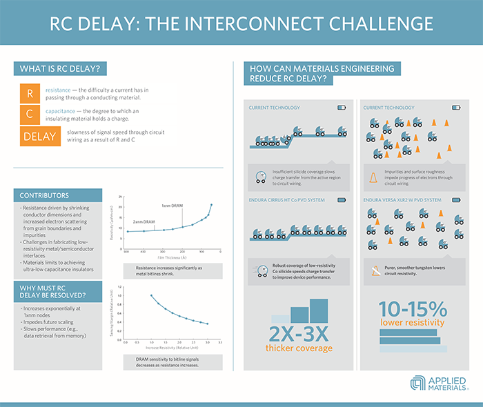
As integrated circuits and their components continue to scale downward, the dimensions of metal interconnects and contacts between components are also shrinking. One result is that the resistance in these connectors is increasing. To achieve more compact, faster electronic devices, resistance must be kept to a minimum so that further scaling is feasible.
The slowing effect produced by this higher resistance is often referred to as resistance-capacitance delay (or RC delay) and affects circuits in a variety of ways. Among its undesirable effects, RC delay can degrade the speed at which data are written to and read from DRAM structures via the bitline. In addition, higher resistance leads to higher power consumption, an undesirable side effect for mobile technologies.
The easiest means of lowering line resistance would be to increase the volume of the conducting metal, i.e., make the wires wider and taller. However, wider wires restrict scaling, and taller wires increase capacitance and pose greater etch challenges. Consequently, lowering wire resistance in leading-edge devices focuses on improving the properties of the conducting material, tungsten (W) in case of DRAM bitlines.
The resistance of a conductor is a function of the density of scattering sites encountered by electrons as they move through it. Impurities in the film, grain boundaries, and surface roughness are some of the impediments that slow the electrons down. The Versa XLR2 W PVD chamber reduces interconnect resistance by depositing purer and smoother tungsten film with resistivity 10-15% lower than tungsten deposited using current technology.
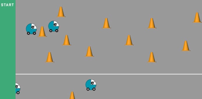
The new system achieves this enhanced quality by means of innovations to key hardware components, such as the source magnetron; novel process chemistry; and modulation of plasma characteristics. A scaling enabler, the lower-resistance tungsten produced by the Versa XLR2 W system will extend the use of tungsten as the bitline metal in DRAM technology for 1xnm nodes. The animation below explains how the system’s superior film improves device performance..
RC delay is important because it can become a significant obstacle to continued downward scaling of logic and memory devices that drive the performance of today’s multi-functional, mobile consumer electronic devices.
Active devices (transistors) in both logic and memory chips are electrically connected to each other and other areas of the chip with metal wiring. These wires are separated from each other using non-conducting (insulating) dielectric layers. In both logic and memory, the role of interconnects is to transmit signals from one area of the chip to another. The ability to do this as rapidly as possible, while minimizing signal losses in shrinking geometries, is critical for device scaling.
In logic, scaling implies area scaling, that is packing more and more circuits into a smaller area by means of materials and design innovations. In price-sensitive DRAM fabrication, costs must be aggressively controlled, so scaling focuses on obtaining progressively better performance from existing materials and design.
In general, the speed of signal propagation in logic and memory wires is governed by the same basic principles and depends on the product of resistance and capacitance (RC). Lowering both resistance and capacitance would be ideal. However, the costs of developing and integrating lower-capacitance insulating materials into the fabrication flow are especially high for memory manufacturers. Lowering resistance is therefore the preferred approach for scaling performance.
Different solutions are needed to address the RC challenge, depending on whether the charge travels vertically across different levels of wiring or laterally along the length of the conductor. In either case, though, the goal is to minimize the resistance of the metal wiring.
In the vertical dimension, solutions are aimed at minimizing interface resistance. Electrical contacts connect the active region of the device to the first level of metal wiring. A semiconductor-to-metal interface (or Ohmic contact) forms the junction between the active region and the metal contact. The objective is to ensure that an electrical charge can travel from the active region through the contact to the upper levels of wiring, and back again. To achieve rapid and maximal charge transmission across the Ohmic contact, a low-resistivity material is formed. Low-resistivity Co silicide has been adopted as the industry standard for this purpose; its effectiveness relies on the deposition of a uniform layer to form a robust Ohmic contact. See ENDURA CIRRUS HT Co PVD.