Products & Technologies
Products & Services
Company
Contact
Products & Services
Products & Technologies
Services
Resources
Company
Contact
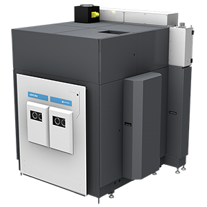
Centura® Epi 200mm
Responding to evolving power and MEMS device requirements, device manufacturers are targeting thicker epitaxial layers. Film thicknesses up to 150µm and tighter fabrication tolerances for Rs (sheet resistance), defect density, thickness uniformity, and particle performance are causing the market to move away from batch toward single-wafer processing.
The Applied Centura Epi system is a production-proven, single-wafer, multi-chamber epitaxial silicon deposition product. Each radiantly-heated process chamber delivers precise and repeatable control of deposition conditions and 100% slip free films, excellent film thickness and resistivity uniformity, and low defect levels. The system’s wide range of temperatures and pressures, excellent temperature uniformity, and flexible gas panel configurations enable advanced low-temperature epitaxial and polycrystalline deposition processes, including germanium and silicon-germanium. In addition, the ability to configure up to three process chambers and hardware optimized for superior in-situ chamber cleaning deliver market-leading throughput density and low cost of ownership.
Applied’s 200mm Centura Epi platform can now be configured with a Siconi pre-clean chamber. The pre-clean technology has been developed to address the increasing demand for a low-temperature epi process on legacy CMOS nodes, driven by emerging applications like RF and photonics. Siconi pre-clean technology enables low-temperature native oxide removal, thereby reducing the thermal budget of the epitaxial process and mitigates the process variability caused by queue time variation.
Applied offers two epi technologies: Atmospheric (ATM) for thin and thick blanket films and Reduced Pressure (RP) for trench fill applications. Complementing Applied’s existing ATM and RP epi chambers, the Centura Pronto™ ATM Epi high-growth-rate chamber enables growth of thick and thin films in a single 150/200mm chamber (<20μm to 150μm in a single pass) with high productivity and 6μm/minute growth rate. This system improves on-wafer performance by increasing center-to-edge uniformity and wafer-to-wafer repeatability.