Products & Technologies
Products & Services
Contact
Products & Services
Products & Technologies
Services
Resources
Contact
Posted
January 26, 2024

Stay updated on our content.
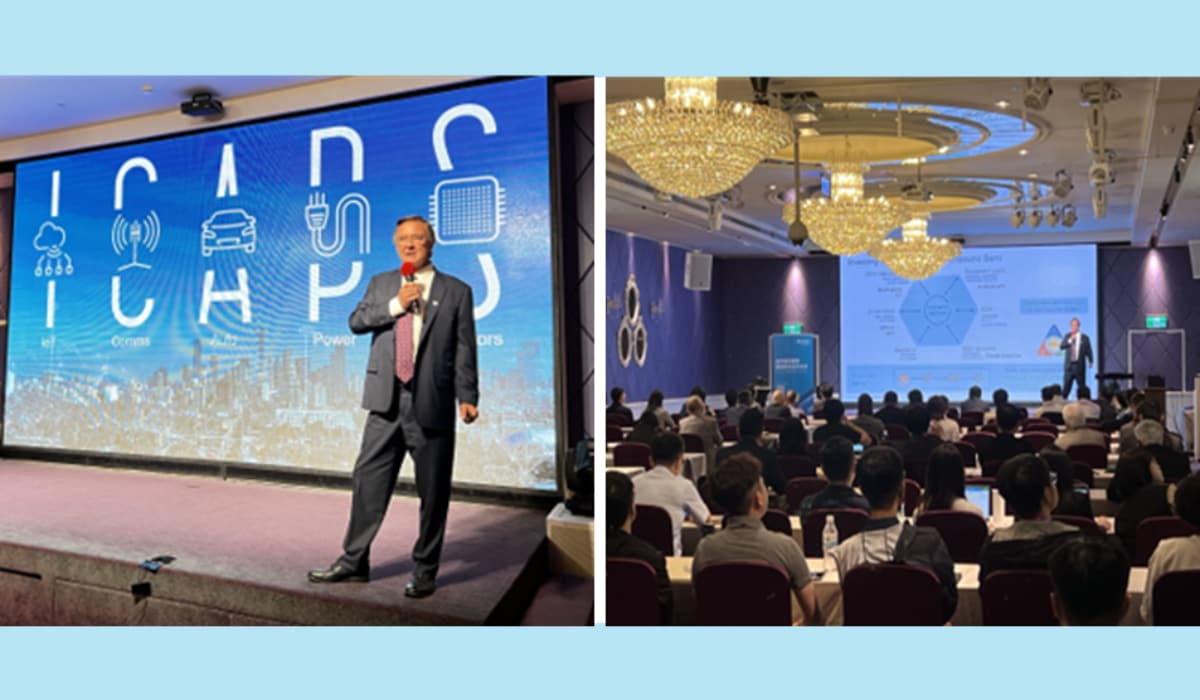
What’s Driving the Need for Innovation in ICAPS?
by Aninda Moitra
January 26, 2024
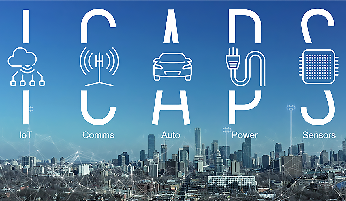
Applied Materials reached a significant milestone in 2023: For the first time, the largest portion of our wafer fab equipment sales came from customers in markets related to ICAPS – IoT, Communications, Automotive, Power and Sensors. Whereas customers in the leading-edge foundry-logic segment use the most advanced process technologies, for primarily digital applications, ICAPS customers leverage mature or highly specialized process technologies to manufacture a wide range of devices.
Historically, about two-thirds of foundry-logic sales were for the three leading nodes, and around one-third were for mature nodes. In 2019, we saw the landscape shifting and formed a horizontal business unit focused on ICAPS to serve the unique needs of customers across these specific vertical markets. Since then, ICAPS has grown significantly, driving around one-half of foundry-logic sales.
Some have been surprised by the growth in ICAPS, but we have seen several trends that support ICAPS as a strategic growth market. Historically, a significant portion of ICAPS demand was fulfilled by used equipment, sold at a discount to new tools. The steady growth in demand for ICAPS chips, driven by powerful megatrends, absorbed the used equipment market, thereby increasing new equipment sales. Going forward, ICAPS will continue to be fueled by large, global inflections that will play out over the next decade. The Internet of Things (IoT) and the clean energy revolution are two of the key megatrends. In this blog, I will explain why these trends are driving the need for materials innovation in a variety of ICAPS applications, from mature logic chips to power electronics.
Two Sides of the Same Coin
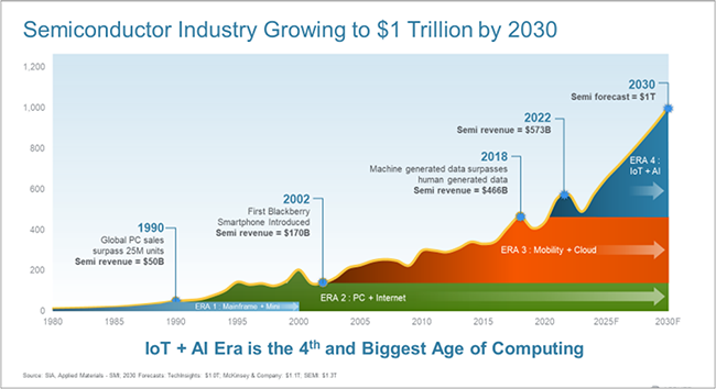
At Applied, we believe that 2018 was the beginning of a new era of computing, in which IoT and artificial intelligence (AI) would team up to create a new wave of growth for semiconductors. This is the year that marked the transition from an app-centric world, focused on people creating data, to a data-centric world, where machines generate more data than people do.
IoT extends internet connectivity beyond typical computing devices – such as desktops, laptops, smartphones and tablets – to a wide range of physical devices and everyday products that have not typically been internet-enabled. Embedded with technology, these devices can now communicate over the internet while being remotely monitored and controlled. IoT devices have both industrial and consumer uses. We are seeing rapid growth in IoT at the edge, with the number of global connected IoT devices predicted to reach nearly 30 billion by 2027[1]. These devices span multi-billion-dollar markets such as automotive, industrial, smart home, wearables and healthcare.
IoT devices on the edge generate data which then gets routed to the cloud, where data centers use leading-edge logic and memory to make sense of the data using AI. This sets up a virtuous cycle for semiconductors whereby the IoT chip markets fuel the markets for leading-edge logic and memory. This is why we call IoT and AI “two sides of the same coin.”
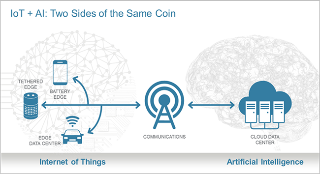
However, IoT is by its nature much more diverse and complex. If advanced logic and memory are like the brains of a computing system, then IoT devices are like the eyes, ears, nose and skin. To digitize the world around us, we rely on analog-to-digital circuitry to interface with computers. At the heart of these new connected devices are a variety of semiconductors – embedded processors, RF communication chips, power modules, CMOS image sensors, MEMS devices, photonics chips and a whole host of specialty components that help our devices sense the analog world, compute locally or in the cloud, and translate information back to us using analog sensors.
IoT devices are manufactured across a wide range of process nodes beyond the leading edge. While these processes have been in production for years – and in some cases, even decades – there is still a tremendous amount of innovation needed to enable differentiated devices for IoT applications. Whether commercial or consumer, we all want devices with the best performance, lowest power for longer battery life, smaller area for size and weight, all at the lowest possible cost.
As an example, consider the emerging Bluetooth® Low Energy (BLE) communications protocol. Global IoT connectivity is dominated by three key technologies: cellular, Wi-Fi and Bluetooth. About one-third of global IoT connections rely on Bluetooth, with the BLE category being developed in recent years to allow IoT devices to maintain reliable connectivity while consuming limited power[1]. As a result, BLE is now a preferred option for battery-powered IoT devices. Driven by continued strong growth in peripheral devices, BLE single-mode device shipments reached 1.5 billion in 2023 and are forecasted to more than double over the next five years[2]. To support this tremendous growth and need for innovation, BLE chip designers and their foundry partners are developing new RF-optimized versions of their existing manufacturing processes, across mainstream nodes such as 28nm, 22nm and 16nm. These optimized process nodes are, in turn, driving the need for innovation in ICAPS process equipment.
A Green Revolution
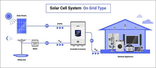
Another key megatrend is the clean energy revolution, driven primarily by broad global transitions to electric vehicles, renewable energy and smart grid technologies.
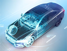
As vehicles shift from internal combustion engines to electric power, the battery becomes the centerpiece of the ecosystem. Instead of filling up with gas, you fill up your battery at a charging station. When the battery discharges, it goes through a power conversion, which requires a power inverter in the vehicle. Each of these situations requires specialty power semiconductors with unique performance requirements due to the extreme operating ranges. Compared to a gas-powered car, an electric vehicle with advanced driver assistance systems is estimated to require about four times the semiconductor content measured in dollars[4].
At the same time, a profound change has been occurring in how electricity is generated, delivered and used. To deliver power from a gas or steam turbine to the grid, there is very little semiconductor content required. It’s basically direct alternating current generation that gets fed directly onto the grid. But the situation is different when you have a renewable source. For example, solar panels generate direct current that needs to be converted to alternating current. Wind generates alternating current, but the phase of the alternating current needs to be synchronized with the grid. This power conversion drives a tremendous amount of semiconductor content.
At the heart of this transition lies the power semiconductor device, which modulates the electrical energy flow to suit the demands of a wide variety of applications. Power electronics cover a large family of device types, from thyristors to trench MOSFETs. Many of these devices are built on silicon today, and there is a great deal of innovation needed to continue scaling silicon power electronics for emerging applications.
At the same time, compound semiconductors are generating a new wave of excitement in the industry. Composed of chemical elements belonging to two or more different groups in the periodic table, compound semiconductors have unique material properties that enable high-speed and high-power devices that operate at higher voltages and consume a fraction of the energy. Wide bandgap semiconductor materials such as silicon carbide (SiC) and gallium nitride (GaN) are increasingly being evaluated and adopted for applications in electric vehicles and power conversion. Because these materials have dramatically different properties than silicon, new manufacturing techniques and processing equipment are required to bring these promising technologies to high-volume production.
Materials Matter
While ICAPS markets and applications are wide-ranging and diverse, they have one thing in common – progress is often driven by innovations in materials engineering, not by shrinking the size of features in the transistor or wiring stack. And while many in the industry still describe these as “trailing nodes” and “legacy nodes,” these terms miss the renaissance in materials innovation that’s happening in the ICAPS markets. Innovation is happening across multi-dimensions: new materials, new architectures and new wafer sizes.
Of course, materials engineering is Applied’s core capability. We are the market and technology leader in materials engineering, and this puts us in a great position to advance our ICAPS customers’ technology roadmaps. Since launching our ICAPS business, we have introduced more than 20 new products for the segments supporting ICAPS devices. ICAPS is a solutions business: our teams are focused on the end markets, working with leading customers to create innovations based on Applied’s full portfolio, including co-optimized and integrated solutions.
We are also investing in collaborative R&D to enable faster time to innovation for ICAPS chipmakers, such as our recently announced joint lab with CEA-Leti. Projects at the joint lab will focus on developing solutions for a variety of materials engineering challenges to enable the next wave of ICAPS device innovation.
This is only the beginning. Stay tuned for more exciting news from Applied about steps we are taking to further accelerate ICAPS innovation.
1 https://iot-analytics.com/number-connected-iot-devices/
2 https://iot-analytics.com/number-connected-iot-devices/
3 https://www.bluetooth.com/2023-market-update/
4 Infineon ATD report, 2015, 2020
Aninda Moitra
Corporate Vice President, General Manager – ICAPS Business Unit

Aninda Moitra is Corporate Vice President and General Manager of Applied’s ICAPS business unit, which provides the broadest products and materials engineering solutions for customers in the Internet of Things (IoT), Communications, Automotive, Power and Sensor markets. During his nearly 30 years at Applied, Aninda has held a variety of business management and new business development positions and served as country president of Applied Materials India. He holds an MBA from Columbia Business School and a bachelor’s degree in chemical engineering from the University of Minnesota.
Q&A: Galvanizing the Ecosystem to Drive Innovation in Compound Semiconductors
Applied Materials recently hosted a Compound Semiconductor Forum in Taiwan with leaders from across the manufacturing ecosystem. We sat down with David Britz, Senior Director of Strategic Marketing for Applied’s ICAPS Business, to learn more about the event and how Applied is enabling the next era of innovation in this exciting field.
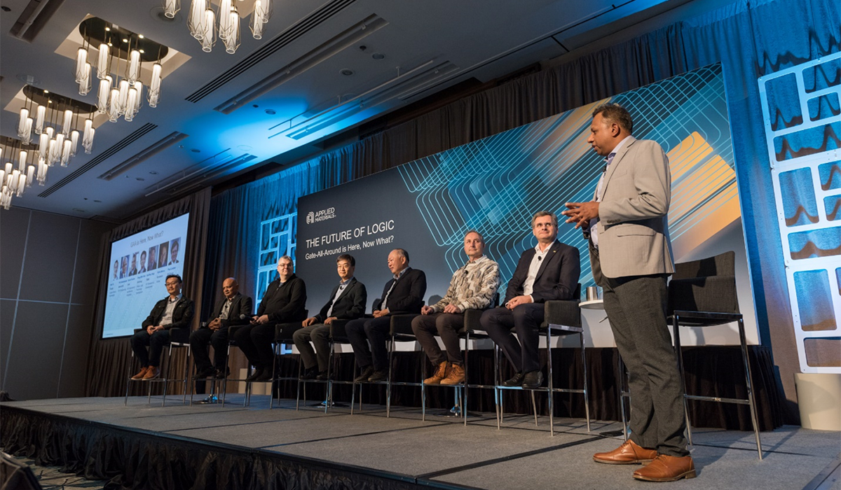
Charting a Course Through the Next Era of Technology Inflections: Applied Materials’ Panel During IEDM 2023
Applied recently hosted a thought-provoking panel during IEDM in San Francisco titled, “The Future of Logic: Gate-All-Around is Here, Now What?” In a wide-ranging discussion, technology leaders from Google, Qualcomm, Intel, Samsung, TSMC, Synopsys and EV Group offered their perspectives on the disruptive innovations that will drive semiconductor growth in the AI era.

Revisiting the Future of Logic at IEDM 2023
Applied is showing up in full force at the 2023 IEEE International Electron Devices Meeting (IEDM). In addition to presenting at important conference sessions, Applied will be hosting a thought-provoking panel discussion featuring leading technologists from Google, Qualcomm, Intel, Samsung, TSMC, Synopsys and EV Group.