Products & Technologies
Products & Services
Contact
Products & Services
Products & Technologies
Services
Resources
Contact
Posted
January 15, 2021

Stay updated on our content.
Trends Accelerating the Semiconductor Industry in 2021 and Beyond

Jan 15, 2021
In adapting to the challenges of COVID-19, the world has experienced profound societal, economic and technological changes that are redefining nearly every aspect of our lives. New capabilities underpinned by the Internet of Things (IoT), 5G and AI are providing a digital lifeline for millions of people by enabling virtual workspaces, remote education, a thriving e-commerce marketplace and a host of other communication and collaboration tools.
The dependency between the global economy and technology is greater today than it’s ever been, and this is creating sustained demand for semiconductors. It is also broadening the growth drivers for the semiconductor industry. While consumer devices led electronics demand over the past decade, commercial investments in IoT, Big Data, AI and 5G infrastructure are poised to lead the next decade and reshape every industry on the planet, from pharmaceuticals and healthcare to agriculture, energy and transportation.
Among all of the emerging technology megatrends, AI in particular has major implications for the electronics and semiconductor ecosystem. First, we’re moving from an application-centric world to a data-first model where almost all data will be generated and consumed by machines. This means that the industry’s growth will no longer be limited by the ability of humans to create or consume data.
Second, a new computing approach is needed to make sense of the massive volumes of available data. We’ll enhance productivity using faster, workload-specific hardware built from customized, and even entirely new, types of silicon. And third, training neural networks for AI computing is incredibly energy intensive, which places a huge imperative on the industry to drive performance-per-watt improvements.
Applied Materials believes the rise of AI and the data economy are fueling a new era of growth for chipmakers and the semiconductor equipment industry. We are seeing the end of a decline in equipment capital intensity that took place from 2000-2013 as the productivity enhancements of 300mm wafers, fab automation and chipmaker consolidation curtailed equipment sales growth. During that period, equipment capital intensity declined from 17% to only 9%, leaving equipment sector revenue capped at around $35 billion per year at various peaks.
Today, equipment capital intensity has returned to the 40-year average of around 12%, and equipment revenue is once again growing in line with the chip sector. By 2030, forecasters expect the semiconductor industry to reach $1 trillion, and if the equipment market tracks its growth, WFE spending will increase from nearly $60 billion in 2020 to more than $100 billion in 2030, with cyclical growth punctuated by higher highs and higher lows.
As we enter what we believe will be an unprecedented period of industry expansion in the decade ahead, the traditional driver of chip technology progress—classic Moore’s Law scaling—has run out of steam and can no longer provide simultaneous improvements in power, performance and area-cost (PPAC). This is causing the industry to adopt a new playbook for achieving PPAC gains to unlock the potential of IoT, Big Data and AI. This new playbook is defined by new semiconductor architectures, 3D structures, novel materials, new ways to shrink features and new ways to connect individual chips with advanced packaging. A most important consideration for chipmakers in a world of rising fab costs is time to market—the “t” in Applied’s PPACt framework.
Applied Materials is uniquely positioned to accelerate the new PPACt playbook for our customers. We have the largest portfolio of technologies to create, shape, modify, analyze and connect chip structures and devices. The breadth of our portfolio is a key advantage because it allows us to combine technologies in innovative new ways to partner with our customers and create long-term value and growth.
The advances in technology needed to accelerate AI and the digital economy create tremendous opportunities for Applied Materials. We’ve aligned our strategy and investments around this vision of the future and look forward to bringing more technology breakthroughs to the industry in 2021 and the exciting decade ahead.
Tags: iot, 5G, AI, Big Data, digital economy, Moore’s Law, New Playbook, PPAC, WFE
Dr. Raman Achutharaman
Group Vice President and General Manager, Etch and Selective Products Business Unit

Dr. Raman Achutharaman leads the Semiconductor Products Group in defining the technology roadmap; developing the strategic plan to strengthen Applied’s leadership in core wafer fabrication equipment markets; and communicating the vision, strategy, and success to stakeholders. Previously, as general manager of the Etch and Selective Products business unit, he led development and commercialization of the Sym3 Etch system that grew etch revenue from less than $400M to over $2B and gained more than 15 pts of conductor etch market share. Earlier, as general manager of the RTP group, he led development of the Vantage Radiance system, the basis of Applied’s leadership in thermal processing. He received his undergraduate degree in metallurgical engineering from the Indian Institute of Technology, Chennai, and his Ph.D. in materials science and engineering from the University of Minnesota.
Now is the Time for Flat Optics
For many centuries, optical technologies have utilized the same principles and components to bend and manipulate light. Now, another strategy to control light—metasurface optics or flat optics—is moving out of academic labs and heading toward commercial viability.

Seeing a Bright Future for Flat Optics
We are at the beginning of a new technological era for the field of optics. To accelerate the commercialization of Flat Optics, a larger collaborative effort is needed to scale the technology and deliver its full benefits to a wide range of applications.
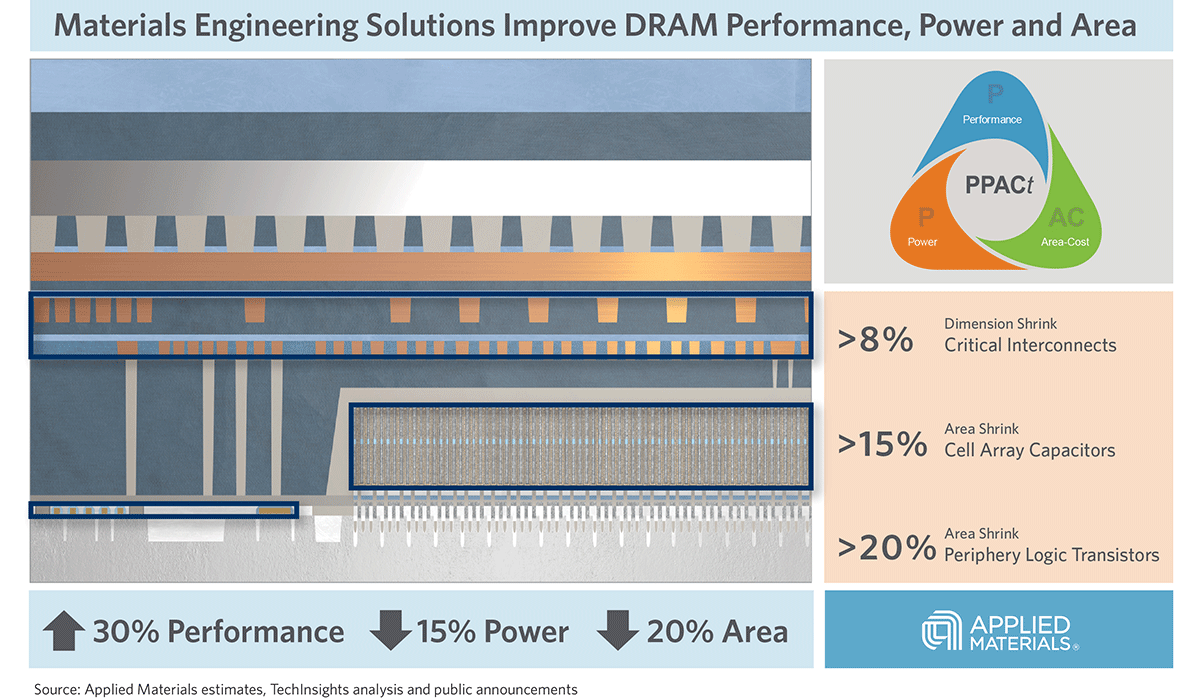
Introducing Breakthroughs in Materials Engineering for DRAM Scaling
To help the industry meet global demand for more affordable, high-performance memory, Applied Materials today introduced solutions that support three levers of DRAM scaling.