Products & Technologies
Products & Technologies
Services
Resources
Posted
August 01, 2024

Stay updated on our content.
Materials Engineering: The True Hero of Energy-Efficient Chip Performance
by Po-Wen Chan and Balaji Chandrasekaran
August 1, 2024
At imec’s 2024 ITF World conference, AMD CEO Lisa Su articulated a vision for a hundredfold improvement in compute power efficiency by the 2026-2027 timeframe, and said, “Driving performance gains over the next decade requires relentless focus on energy efficiency.” The emphasis on delivering energy-efficient compute extends well beyond AI servers to the PCs and smartphones we use every day. As Qualcomm has noted, “Once an AI model is trained, it can be reduced and optimized to run on a significantly less power-hungry piece of hardware, like a smartphone or battery-powered laptop.”
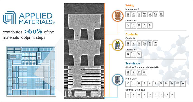
To better understand the impact of materials engineering on the semiconductors powering our digital world, we analyzed one of the most advanced microprocessors available today[1]. Based on a leading-edge 3nm FinFET technology, about 1,900 individual process steps are used to manufacture the chip. Our analysis found that only about 300 of these steps actually leave a materials footprint on the chip, while the rest are associated with defining patterns, cleaning, polishing, measuring, and inspecting the wafer for defects.
And yet, the relatively small number of materials engineering steps have an outsized impact on the performance, power and reliability of the chip. Furthermore, our analysis revealed that more than 60 percent of the materials engineering steps were performed on Applied Materials equipment.
Materials Matter More to Chip Performance
While the semiconductor industry is famous for its ability to continually shrink the critical dimensions of transistors according to Moore’s Law, 2D scaling is delivering diminishing returns. As we run up against fundamental physical barriers, dimensional scaling no longer produces simultaneous improvements in performance and power consumption.
That’s why we need materials innovations. The materials we use and the unique ways we deposit and shape the hundreds of layers of materials at the nano scale increasingly determine chip performance and power consumption.
This is analogous to building a house. An architect defines the lengths, widths, angles and other dimensions that form the layout of the building – this is akin to design and lithography. The building inspector makes sure everything is up to code, with no significant defects – that’s like process control. Ultimately the quality of the materials and construction determine the functional performance, reliability and longevity of the structure – that’s what materials engineering is all about.
Specifically, after lithography, many complex steps are used to “construct” the various chip features that form the transistors and interconnect wiring. Intricate process technologies are used to add, shape, remove and modify a range of exotic materials – at dimensions that can be on the scale of just a few individual atoms and molecules.
Increasing Complexity Drives Innovative Solutions
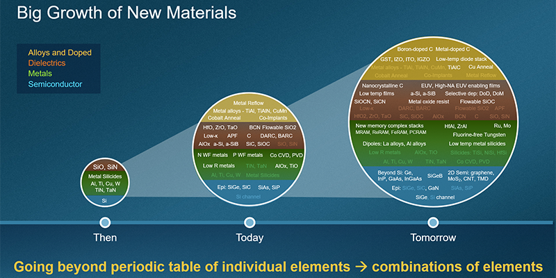
In the early days of the industry, integrated circuits only used about eight elements from the periodic table, and construction was mostly 2D. Today, the industry is adopting more materials that have unique and sometimes exotic physical and chemical properties, and construction is increasingly 3D. To create the most advanced chips, more than 25 elements are combined in 100 different ways. As Intel CEO Pat Gelsinger has said, “Intel remains inspired by Moore’s Law, and we will pursue it until the periodic table is exhausted!” Applied is aggressively exploring candidate elements from the periodic table for future chip technology.
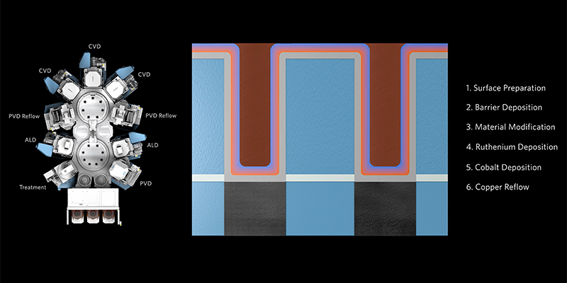
Let’s look at one recent example involving the copper wires that form the electrical connections between the tens of billions of transistors on a chip. A leading-edge processor can contain more than 60 miles of wiring in a chip the size of a fingernail. To create the tiny wires, ultra-thin liners are deposited along the walls of trenches that are later filled with conductive copper. Thinning the liners to make more space available for copper can dramatically reduce the resistance of the wires, resulting in better chip performance and power efficiency. Described in this video animation, Applied Materials’ latest IMS™ (Integrated Materials Solution™) system uses materials innovation to extend copper to the 2nm node and beyond. The system combines six process technologies in one high-vacuum system and uses an industry-first combination of ruthenium and cobalt (RuCo) to simultaneously reduce the thickness of the liner by 33 percent to 2nm. The materials engineering solution improves surface properties for void-free copper reflow which helps reduces electrical line resistance by up to 25 percent.
This is just one example of how materials engineering is complementing 2D scaling to enable continued improvements in performance and power. Applied has the industry’s broadest portfolio of materials engineering solutions across the steps required to create, shape, modify, analyze and connect materials at the atomic scale. We are the leader in materials engineering solutions that make up almost every chip in the world.
Looking to the future, chip nodes and features will be described in angstroms, or tenths of a nanometer. At these dimensions, materials behave in entirely different ways as surface properties begin to dominate bulk properties. Applied has a big role to play in delivering innovative materials engineering solutions that enable customers to continue building high-performance, energy-efficient chips for AI and the next-generation of electronics applications.
[1] TechInsights, April 2024, APL1V02 A17 Pro Processor 3nm report, Applied Materials analysis
Po-Wen Chan
Senior Director, Semiconductor Products Group

Po-Wen Chan is a Senior Director with the Technology Solutions Roadmap team in the Semiconductor Products Group at Applied Materials. He is involved in foundry/logic technology roadmaps and fabless company engagements. Po-Wen earned his master’s degree in chemical engineering from National Taiwan University, and he holds over 20 U.S. patents.
Balaji Chandrasekaran
Vice President, Strategy and Marketing, Semiconductor Products Group

Balaji leads the strategy and marketing group driving long-term planning and strategic growth initiatives at Applied Materials. He holds a bachelor’s degree in metallurgical engineering from the Indian Institute of Technology, Madras, a master’s degree in materials science from Northwestern University and an MBA from the University of California at Berkeley.

The Race for AI Leadership is Fueled by Materials Engineering
At Applied Materials, we believe AI is the single biggest inflection of our lifetimes. However, the compute power required to support the growth of AI is driving energy consumption to new levels. Power is becoming a much more important variable, and we expect the demand for more power-efficient solutions to intensify. To achieve the full potential of AI, we must limit the growth in energy required to train new AI models.
Beyond Backside Power: Scaling Chips to 2nm and Beyond Also Requires Frontside Wiring Innovations
Today’s advanced logic chips have as many as 20 layers of metal that support two types of wires – thin signal wires that switch transistors on and off, and thicker power wires that deliver the current that flows when the transistor is switched on. In the near future, all of the world’s leading chipmakers plan to move the power lines to the backside of the wafer, which promises to reduce wiring complexity, free up space for more transistors, and improve chip performance and power efficiency.
Wafer Fab Equipment Positioned for a New Wave of Growth
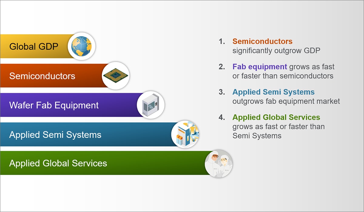
At Applied Materials’ 2021 investor meeting, we suggested that the semiconductor industry had transitioned into a fourth major era of computing. This new “IoT + AI” era began in 2018, when machines generated more data than humans for the first time, complementing the markets for PCs and smartphones that defined the second and third computing eras. Each era creates a new wave of growth by effectively doubling the size of the industry, putting us on track to reach $1 trillion by the end of the decade, as suggested by multiple third-party forecasts.
