Products & Technologies
Products & Services
Contact
Products & Services
Products & Technologies
Services
Resources
Contact
Posted
July 14, 2022

Stay updated on our content.
Takeaways from Panel Discussion at Sustainability Summit
July 14, 2022
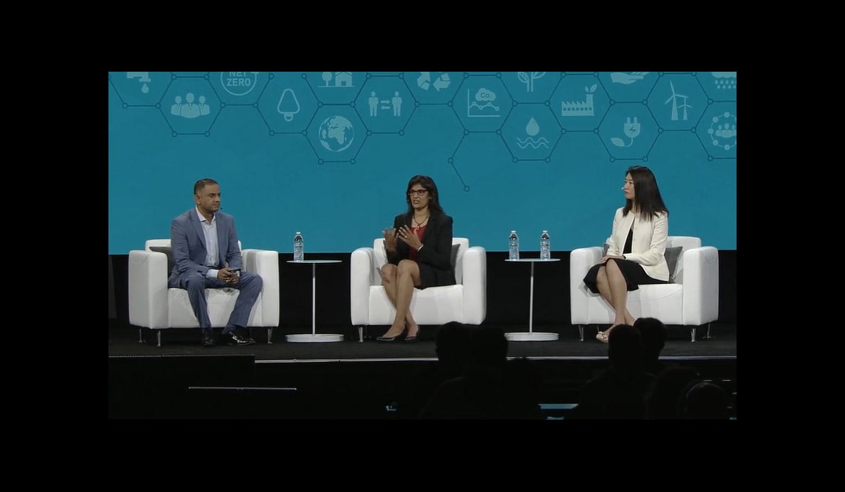
I enjoyed hosting a panel discussion with my colleague Nasreen Chopra, who leads the Systems Engineering Center of Excellence for Applied’s Semiconductor Products Group, and Betty Jiang, head of U.S. ESG Research at Credit Suisse, as part of the Semicon West Sustainability Summit, within Applied CEO Gary Dickerson’s keynote session. I’d like to highlight three key takeaways from the panel.
Takeaway 1: Scope 3 emissions are a large part of our carbon emissions value chain.
The Greenhouse Gas Protocol (GHG Protocol) offers companies different levels of commitments to advance their sustainability journey. For Applied, Scope 1 and Scope 2 cover emissions from the company’s direct operations and indirect emissions due to purchased electricity, respectively. Scope 3 represents 99% of Applied’s carbon emissions footprint for semiconductor products, of which nearly 80% is driven by the use of Applied’s products within semiconductor fabs to make chips. About 15% of Applied’s Scope 3 emissions for semiconductor products originate from supplier inputs. See chart 1 for Applied’s carbon emissions value chain.
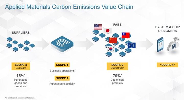
Chart 1: Applied Materials Carbon Emissions Value Chain. Source: Applied Materials - Strategy & Market Intelligence.
System and chip designers determine what types of chips are needed to meet workload and application computing requirements. System and chip designers together with fab operators decide the manufacturing technology (aka “process node” or “technology node”) to be used for high-volume manufacturing of specific chips. They also decide which particular fabs will be used to make those chips. Depending on where a fab is located geographically, it may or may not have adequate access to clean energy for its operations. Carbon emissions due to fab operations represent the fab’s Scope 1 and Scope 2 footprint, and the portion attributable to Applied’s products within the fab drives Applied’s Scope 3 footprint.
Like the writers of the GHG Protocol intended, Scope 3 is designed to encourage a “full system” collaborative approach to lowering shared emissions. Ignoring Scope 3 would relinquish big opportunities to collectively transform the carbon footprint of the semiconductor industry.
Takeaway 2: The semiconductor industry needs to take a holistic approach to cut emissions.
Clearly, the entire value chain can reduce its carbon footprint by making smarter choices about chip architectures, manufacturing technology and fab geography through a collaborative approach. We think of emissions avoided through such an approach as Applied’s “Scope 4” emissions. To enable Scope 4 avoided emissions, the industry would need a priori access to data and analytics estimating potential carbon emissions resulting from design, technology and fab choices. Ideally, cross-industry collaboration would allow chip and system designers to iteratively optimize for value chain carbon emissions in addition to PPACt (power, performance, area, cost and time-to-market) considerations.
The concept of Scope 4 emissions would fit within Applied’s 10,000x strategy framework introduced in 2020 (see chart 2).
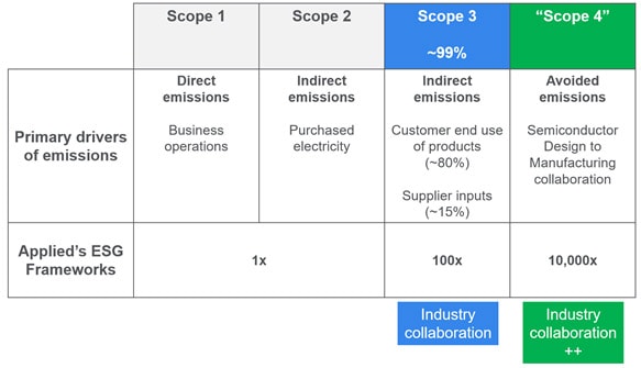
Chart 2: Applied’s ESG Strategy Frameworks. Source: Applied Materials – Strategy & Market Intelligence
A recent Applied blog post provides transparency to how the company has calculated Scope 3 emissions for its semiconductor products and the holistic approach that has been taken. Looking at the details of the Scope 3 calculations, it only becomes more apparent that working across the semiconductor supply chain is critical for this industry to achieve its sustainability targets.
Takeaway 3: Now is the time to take action, while carbon remains mispriced.
Betty’s thesis is that higher carbon prices are needed to accelerate environmental sustainability progress, including innovation and investments in carbon reduction and removal, as well as clean energy generation and the electricity grid. If the semiconductor industry waits for more stringent government policy before taking meaningful actions on environmental sustainability, carbon prices would likely shoot higher by multiples of what they are today. Given the complexity of industry-wide collaboration needed to reduce value chain emissions, the industry would be better served by starting now, while carbon prices remain lower than they should be to meet science-based targets.
I look forward to sharing more of our thinking and progress as Applied advances its sustainability journey.
Tags: sustainability, ES , semiconductor, GHG, Greenhouse Gas Protocol, Scope 3, Scope 4, Semicon West
Sundeep Bajikar
Corporate Vice President, Corporate Strategy and Marketing
Sundeep is Head of Corporate Strategy and Marketing (CSM) and guides the executive leadership team in the development of the company's growth thesis, strategic priorities, key initiatives and investor communications. He is also responsible for developing Applied’s marketing capabilities and community. Sundeep’s work served as the foundation for Applied’s strategies related to AI, ICAPS, Heterogenous Integration and Net Zero.
He joined Applied in 2017 after spending ten years as a Senior Equity Research Analyst covering global technology stocks, including Apple and Samsung Electronics, for Morgan Stanley and Jefferies. Previously he worked for a decade as a researcher, ASIC design engineer, system architect and strategic planning manager at Intel Corporation.
Sundeep holds an MBA in finance from The Wharton School and M.S. degrees in electrical engineering and mechanical engineering from the University of Minnesota. He holds 13 U.S. and international patents with more than 30 additional patents pending. Sundeep is also author of a book titled, “Equity Research for the Technology Investor – Value Investing in Technology Stocks.” He was an Institutional Investor Rising Star.
Classic Moore’s Law Scaling Challenges Demand New Ways to Wire and Integrate Chips
Ever since the earliest days of the computer industry, chip designers have had an insatiable appetite for transistors.
New Ways to Shrink: Further EUV Scaling Depends on Materials Engineering and Metrology Breakthroughs
Traditional Moore’s Law 2D scaling defined the chip industry’s technology roadmap for more than half a century.
Newer Ways to Shrink
In a blog previewing our upcoming “New Ways to Shrink” Master Class, my colleague Regina Freed explained that classic 2D Moore’s Law scaling with EUV can continue well into the future—as long as we also address 6 key issues in materials engineering and metrology.