Products & Technologies
Products & Services
Contact
Products & Services
Products & Technologies
Services
Resources
Contact
Posted
March 14, 2018

Stay updated on our content.
Semiconductor Trends to Watch in 2018

Mar 14, 2018
Major changes are taking shape in the semiconductor industry as a new era of computing emerges centered on artificial intelligence (AI). “Semiconductors and semiconductor processing technologies will play a key enabling role in the AI revolution,” according to Prabu Raja, senior vice president of Applied’s Semiconductor Products Group, who shared his views in Solid State Technology magazine. Prabu sees a broad set of market trends including the Internet of Things (IoT), Big Data, Industry 4.0, VR/AR/MR and autonomous vehicles bringing incredible inflections in new processor architectures, next-generation devices and packaging schemes.
Read Prabu’s full article here and find out how these trends will make 2018 a very exciting year for the semiconductor industry.
Tags: artificial intelligence, AI, Semiconductors
Balaji Chandrasekaran
Vice President, Strategy and Marketing, Semiconductor Products Group

Balaji leads the strategy and marketing group driving long-term planning and strategic growth initiatives at Applied Materials. He holds a bachelor’s degree in metallurgical engineering from the Indian Institute of Technology, Madras, a master’s degree in materials science from Northwestern University and an MBA from the University of California at Berkeley.

Adding Sustainability to the Definition of Fab Performance
To enable a more sustainable semiconductor industry, new fabs must be designed to maximize output while reducing energy consumption and emissions. In this blog post, I examine Applied Materials’ efforts to drive fab sustainability through the process equipment we develop for chipmakers. It all starts with an evolution in the mindset of how these systems are designed.
Innovations in eBeam Metrology Enable a New Playbook for Patterning Control
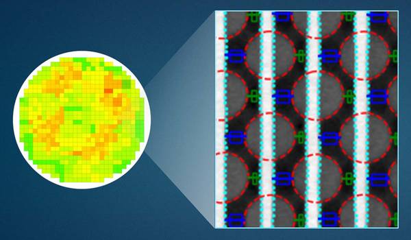
The patterning challenges of today’s most advanced logic and memory chips can be solved with a new playbook that takes the industry from optical target-based approximation to actual, on-device measurements; limited statistical sampling to massive, across-wafer sampling; and single-layer patterning control to integrative multi-layer control. Applied’s new PROVision® 3E system is designed to enable this new playbook.
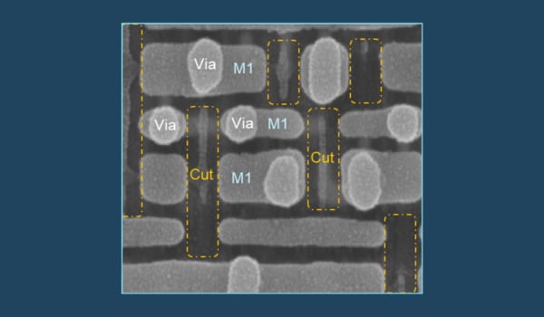
Breakthrough in Metrology Needed for Patterning Advanced Logic and Memory Chips
As the semiconductor industry increasingly moves from simple 2D chip designs to complex 3D designs based on multipatterning and EUV, patterning control has reached an inflection point. The optical overlay tools and techniques the semiconductor industry traditionally used to reduce errors are simply not precise enough for today’s leading-edge logic and memory chips.