Products & Technologies
Products & Technologies
Services
Resources
Posted
April 18, 2019

Stay updated on our content.
New Imaging Technology Speeds Process Development
by Shinsuke Mizuno, Vadim Kuchik
Apr 18, 2019
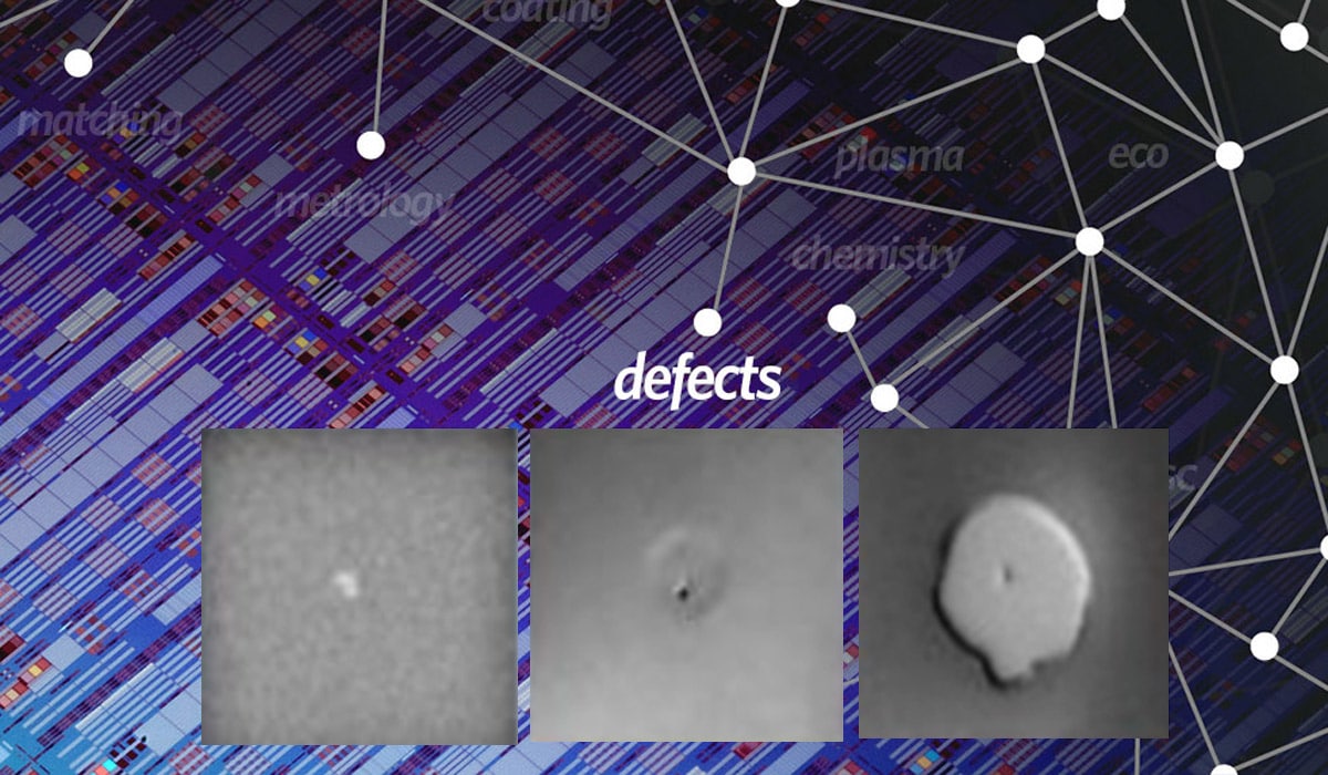
Defects and contamination on the wafer can slow process development times and limit performance and yield. As chips get more complex, more defects can become buried within the increasing number of layers in the design. Finding and analyzing these buried defects is a major challenge for the industry, especially during the early learning cycles of new manufacturing processes. At advanced semiconductor technology nodes, buried voids and foreign materials embedded in films can cause unexpected and unpredictable changes in electrical conductivity.
Fortunately, there is a new eBeam technology that can quickly detect, image and measure critical defects buried within multiple layers of films. Called back-scattered electron imaging, Applied Materials is now enabling the technology in metrology, inspection and review applications.
Detecting buried defects in silicon requires three capabilities. First is being able to penetrate deep into the silicon substrate (Figure 1). Second, once the electrons hit buried defects, they need to have enough energy to escape from the bulk material and return to the detection system (Figure 2). Since the mean-free path of electrons increases with energy, a high-energy beam is required. Third, the resolution needs to be ~1.2 times the defect size. For example, assuming the minimal defect size we want to detect is 100nm, the lowest see-through resolution needs to be approximately 80nm.

Figure 1. Simulation results of penetration depth and different accelerated voltages. We show a correlation between high-energy electrons and defect volume/depth.
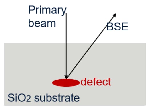
Figure 2. Detecting embedded defects requires a two-way eBeam path to the surface.
Applied’s commercial solution is called Elluminator™ eBeam technology. Today, it is offered on our PROVision™ 2E eBeam inspection system and our SEMVision™ G7 defect review system. We recently demonstrated how the SEMVision G7 system efficiently detects embedded defects and voids using a specially designed detector that enhances detection of high-energy back-scattered electrons.
Better than TEM
A traditional approach to finding buried defects is transmission electron microscopy, a.k.a. TEM. TEM is a slow, destructive method that requires the use of imaging technology to identify where a wafer needs to be cut, ground, polished and ion-milled to produce a defect sample. The TEM analysis cycle usually requires multiple weeks of time and effort.
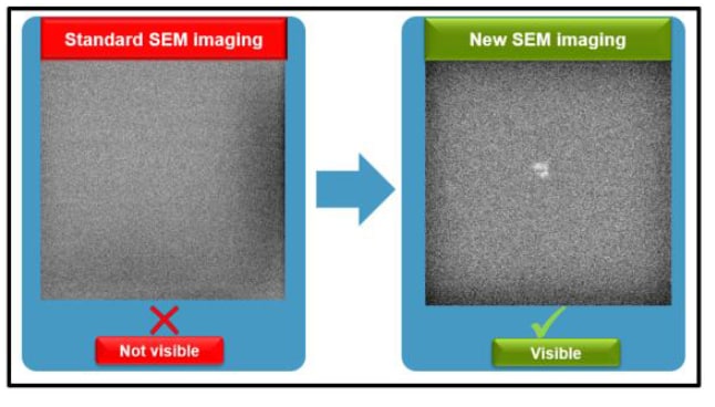
Figure 3. Two images of the same location on a wafer. Standard imaging techniques (left) do not reveal a buried defect. New imaging technology shows the defect (right).
In contrast, back-scattered electron imaging technology pinpoints buried defects and allows them to be quickly imaged in a non-destructive manner (Figure 3). Typical imaging time is less than two seconds, and process quality analysis can be obtained in just hours.
Applied’s Elluminator technology enables massive defect review runs in a fully automatic mode, generating buried defect maps. With it, we are entering a new era of chip performance and yield management.
Tags: eBeam, defect detection
Shinsuke Mizuno
Technologist, Process Diagnostics and Control Group

Shinsuke Mizuno is a technologist with Applied Materials’ Process Diagnostics and Control group supporting a variety of customers. A specialist in yield management, Shinsuke received B.S. and M.S. degrees in organic chemistry from Kinki University, Japan.
Vadim Kuchik
Physicist and SEM Imaging Technologist, Process Diagnostics and Control Group

Vadim Kuchik is a physicist and SEM imaging technologist with Applied Materials’ Process Diagnostics and Control group. He has a M.S. in physics from the Israel Institute of Technology.

Adding Sustainability to the Definition of Fab Performance
To enable a more sustainable semiconductor industry, new fabs must be designed to maximize output while reducing energy consumption and emissions. In this blog post, I examine Applied Materials’ efforts to drive fab sustainability through the process equipment we develop for chipmakers. It all starts with an evolution in the mindset of how these systems are designed.
Innovations in eBeam Metrology Enable a New Playbook for Patterning Control
The patterning challenges of today’s most advanced logic and memory chips can be solved with a new playbook that takes the industry from optical target-based approximation to actual, on-device measurements; limited statistical sampling to massive, across-wafer sampling; and single-layer patterning control to integrative multi-layer control. Applied’s new PROVision® 3E system is designed to enable this new playbook.
Breakthrough in Metrology Needed for Patterning Advanced Logic and Memory Chips
As the semiconductor industry increasingly moves from simple 2D chip designs to complex 3D designs based on multipatterning and EUV, patterning control has reached an inflection point. The optical overlay tools and techniques the semiconductor industry traditionally used to reduce errors are simply not precise enough for today’s leading-edge logic and memory chips.
