Products & Technologies
Products & Technologies
Services
Resources
Posted
August 01, 2018

Stay updated on our content.
Mobile-Centric World Drives New Packaging Trends

by Mike Rosa
Aug 01, 2018
In today’s mobile-centric world, form factor and functionality rule. A major challenge for designers is keeping their products thin and lightweight as more and more chips are added inside. In response to this we are seeing increased use of wafer-level packaging (WLP) for chips used in mobile products. WLP refers to the technologies of packaging an array of integrated circuitry together at the wafer level rather than assembling them into individual packaged units.
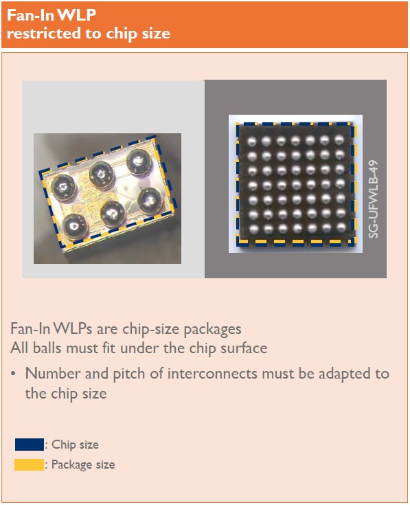
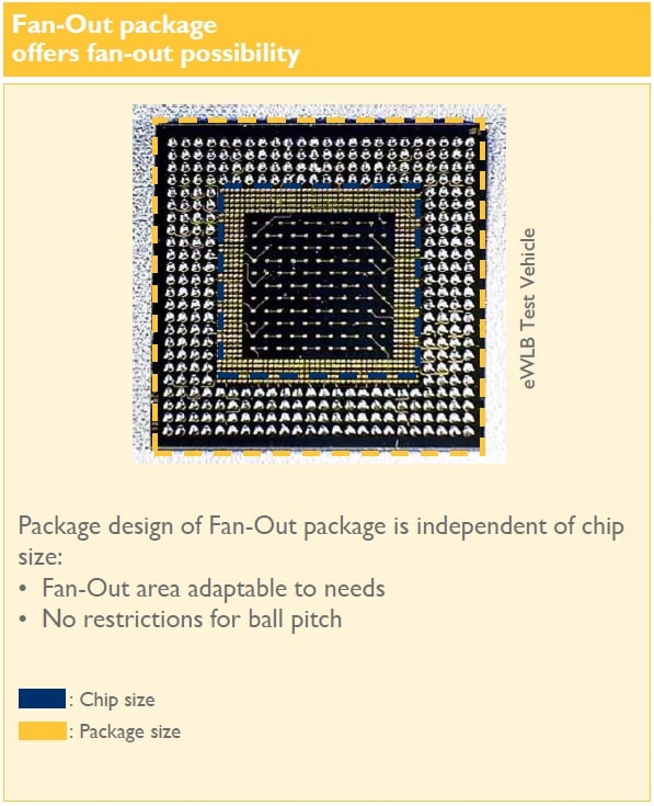
WLP reduces the footprint and overall thickness of the semiconductor content by eliminating the need for wire bonds (and subsequently bond pads). There are a number of WLP schemes (Bump/Pillar, Fan-In, Fan-Out, Through Silicon Via or TSV, and more), but most can be broadly and simply categorized as either Fan-In or Fan-Out technologies. Fan-In schemes apply to both 200mm and 300mm wafer sizes and are used when the required number of pin-outs (or solder ball connections) can fit within the area of the die. Fan-Out schemes are used when the number of pin-outs requires an area greater than that of the original die.
These techniques all extend wafer fab processes utilizing traditional fab tools for building interconnects.


We are seeing demand for WLP integration schemes growing to support the huge variety of More-than-Moore (MtM) device types. Among these, there is a marked increase in volume for micro-electro-mechanical systems (MEMS), CMOS image sensors (CIS), light-emitting diodes (LED), and power management, wireless, analog and mixed signal ICs along with many other technologies.
This mix of MtM devices is driving the roadmaps of leading outsourced assembly and test companies (OSATs) and IDMs to ramp their Fan-In WLP technologies using 300mm tools as well as legacy 200mm equipment. Market research firm Yole Developpement forecasts a >7 percent compounded annual growth rate (CAGR) through 2020 for WLP technologies with an expected market value of more than $30B by 2020.
Applied is helping accelerate the adoption of WLP for 300mm and 200mm wafers by providing innovative solutions that solve several manufacturing challenges. Among these is the capability of the Applied Nokota™ Electrochemical Deposition (ECD) system to ensure a wafer remains completely sealed throughout the plating sequence to protect it from potential damage. The system’s flexible single-chamber design also allows for quick, in-fab reconfigurations between different process flows making it ideal for handling the growing selection of WLP schemes, product mixes and capacity demands.
Applied uses several R&D facilities to enable the WLP inflection. To develop packaging schemes involving TSVs, under bump metallization (UBM) and solder bumps, Applied supports R&D at a facility in Xi'an, China and at our Packaging, Plating and Cleans (PPC) operation in Kalispell, Montana where ECD development and demonstrations are performed. For 300mm WLP processes and solutions, we have a suite of systems installed in the Applied Packaging Development Center located in Singapore.
As the use of WLP technology increases on ≤200mm and 300mm processes alike, more customers are looking for fully-integrated, end-to-end solutions demonstrated on their wafers. Many customers in the power, high brightness LED and MEMS spaces are utilizing the WLP integration processes offered by Applied to develop their own 150mm and 200mm WLP solutions. We are able to help customers shorten their process development time through the capabilities of our systems.
Tags: wafer-level packaging, wafer level packaging, WLP, Advanced Packaging, fan-in, fan-out, electromechanical plating, More than Moore

Mike Rosa

Adding Sustainability to the Definition of Fab Performance
To enable a more sustainable semiconductor industry, new fabs must be designed to maximize output while reducing energy consumption and emissions. In this blog post, I examine Applied Materials’ efforts to drive fab sustainability through the process equipment we develop for chipmakers. It all starts with an evolution in the mindset of how these systems are designed..

Innovations in eBeam Metrology Enable a New Playbook for Patterning Control
The patterning challenges of today’s most advanced logic and memory chips can be solved with a new playbook that takes the industry from optical target-based approximation to actual, on-device measurements; limited statistical sampling to massive, across-wafer sampling; and single-layer patterning control to integrative multi-layer control. Applied’s new PROVision® 3E system is designed to enable this new playbook.

Breakthrough in Metrology Needed for Patterning Advanced Logic and Memory Chips
As the semiconductor industry increasingly moves from simple 2D chip designs to complex 3D designs based on multipatterning and EUV, patterning control has reached an inflection point. The optical overlay tools and techniques the semiconductor industry traditionally used to reduce errors are simply not precise enough for today’s leading-edge logic and memory chips.
