Products & Technologies
Products & Technologies
Services
Resources
Posted
June 12, 2019

Stay updated on our content.
Memory Trends for a New Computing Era

by Sean SK Kang
Jun 12, 2019
The semiconductor industry is on the verge of a transformative computing era driven by Big Data, Artificial Intelligence (AI) and the Internet of Things (IoT). However, achieving the improvements in computing performance and efficiency needed for new AI and IoT applications represent some of the biggest technology challenges the industry has faced.
Among the most critical requirements is delivering on new memory technologies. This was the dominant focus of discussions at the 11th International Memory Workshop (IMW) held recently in Monterey, where leading experts reviewed the latest advances in process and design technologies, applications and market needs for memory solutions.
At a joint CEA-Leti and Applied Materials workshop titled, PCM/MRAM: What to expect/how to manage artificial intelligence, in-memory computing and IoT, distinguished company representatives reported on current challenges, R&D progress and new solutions. Several themes emerged from the presentations; chief among them was the need for more efficient computing as the current trajectory of energy consumption is not sustainable. Also, very different applications and market segments are driving diverse memory requirements, technologies and strategies. And, after years of development and learning, process technologies are ready to support the use of new memory types in commercial applications.
The fundamental driver for today’s industry roadmaps is the explosion of data. By 2022, over 10 zettabytes of data—approximately 90 percent of it machine generated—will need to be processed, stored and transferred. This enormous amount of data reflects the proliferation of more intelligent edge applications such as smart speakers, wearables, industrial sensors and smart vehicles. We’re seeing a buildout of data centers to keep up. The energy appetite of all this processing and data transfer can consume the equivalent of an entire country’s energy supply if left unchecked.
According to one of the speakers, 90 percent of energy consumed by memory is used to transfer data. Moving memory closer to compute can alleviate this. Multiple strategies are being worked on to increase the power and performance efficiency of memory and compute, including memory optimized for edge and storage applications, new system on chip (SoC) packaging schemes, 3D packaging using TSVs, and in-memory compute, which has the potential to deliver an 8X reduction in energy.
No single new memory type can handle all the different requirements of emerging data-generating applications. From the range of emerging memories, MRAM, PCRAM and ReRAM are on their way to achieving the maturity levels for market adoption. Each technology has attributes optimized for various applications—MRAM for the edge and IoT, PCRAM for the cloud—but all will improve performance and energy consumption.
Highlighting the progress achieved for manufacturing emerging memories, my Applied colleagues focused on what it takes to enable some of these technologies, in particular MRAM and PCRAM, into volume production.
For MRAM, the major challenge is the deposition of the memory stack, which is typically done with PVD technology. Atomic-level precision and control are required to deposit over 10 different materials in more than 30 extremely thin layers, some of which can be only a couple of angstroms thick. Damage-free etch and encapsulation are needed to maintain the integrity of the critical, very thin magnetic tunnel junctions.
Like MRAM, PCRAM is enabled by new materials and requires innovations in PVD and etch technology. Being composition-based (consisting of three different elements combined), PCRAM materials tend to be very complex and thickness uniformity is essential. Having process knobs that allow compositional tuning and minimal damage is extremely important to how the materials will change phase. Process technology allows the composition to be tuned for high retention, temperature, high speed or high endurance—depending on the application.
The formation of the material stacks determines the performance of the memory. With the use of so many complex materials, exposure to atmosphere can cause contamination and damage. This necessitates an ultra-high vacuum solution that integrates a variety of process technologies along with metrology to ensure the pristine integrity and control of the materials for the high-volume manufacture of materials-enabled memories.
Tags: emerging memory, MRAM, PCRAM, ReRAM, artificial intelligence
Sean SK Kang
Director, Semiconductor Products Group

Sean SK Kang is a director in the Semiconductor Products Group focused on next-generation inflections and market trends. He has worked on semiconductor technologies for more than 20 years. He holds a Ph.D. in materials science and engineering, and an MBA from the University of Michigan. Sean has published 15 technical papers as first author and holds ~ 30 patents.

Now is the Time for Flat Optics
For many centuries, optical technologies have utilized the same principles and components to bend and manipulate light. Now, another strategy to control light—metasurface optics or flat optics—is moving out of academic labs and heading toward commercial viability.

Seeing a Bright Future for Flat Optics
We are at the beginning of a new technological era for the field of optics. To accelerate the commercialization of Flat Optics, a larger collaborative effort is needed to scale the technology and deliver its full benefits to a wide range of applications.

Introducing Breakthroughs in Materials Engineering for DRAM Scaling
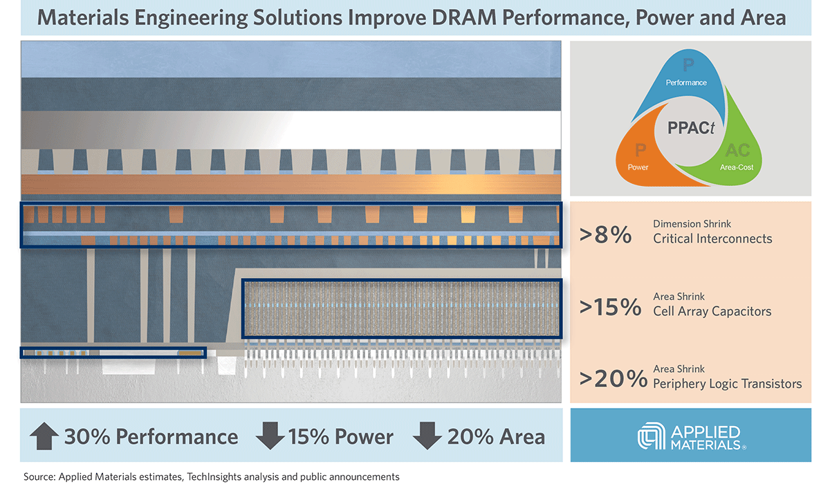
To help the industry meet global demand for more affordable, high-performance memory, Applied Materials today introduced solutions that support three levers of DRAM scaling.
