Products & Technologies
Products & Technologies
Services
Resources
Posted
July 01, 2024

Stay updated on our content.
Materials Innovations Can Help Make Quantum Computing a Reality

By Jake Rochman
July 1, 2024
Quantum computing is a critical technology to enable the next generation of computation power. While it will require advancements across the quantum computing ecosystem, innovations in materials engineering, semiconductor processing and advanced packaging can play a central role.
To help drive collaboration among quantum computing specialists from different backgrounds, Applied Materials recently hosted an Open Innovation Workshop on quantum technology. The workshop provided a forum for discussing new ideas to solve quantum computing’s biggest challenges through focused and open discussion with scientists and engineers across the quantum computing ecosystem.
Quantum Computing 101
Quantum computers use quantum entanglement and quantum superposition of quantum bits (or qubits) as a resource for computation. This crucial feature enables new algorithms that can efficiently solve particular high-value problems, with potential applications including material science, drug discovery, cryptography and machine learning.
There are many different hardware platforms being developed to create qubits for a quantum computer, including systems within solid materials – such as superconducting qubits, spin qubits and color centers – and systems exploiting natural particles such as photonic qubits, trapped ions and neutral atoms.
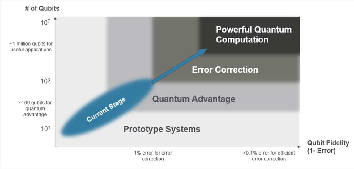
Regardless of the hardware, making a quantum computer that is powerful enough to solve useful problems is extremely difficult. It requires building a system that contains a large number of qubits while maintaining extremely low gate error rates. Both attributes require orders of magnitude improvements beyond what is currently possible today.

References: Fowler, Austin G., et al. "Surface codes: Towards practical large-scale quantum computation." Physical Review A—Atomic, Molecular, and Optical Physics 86.3 (2012): 032324. Arute, Frank, et al. "Quantum supremacy using a programmable superconducting processor." Nature 574.7779 (2019): 505-510.
There has been significant progress in the hardware development of quantum computers over the past decade, where they have emerged out of academic research labs and into companies with dedicated quantum computing efforts. Current systems using different hardware have used more than 100 qubits and demonstrated error rates under one percent. Importantly, the error rates are near the threshold where quantum error correction can enable the suppression of native errors – a critical milestone to achieve the low error rates required to make a useful quantum computer.
Additional hardware improvements are needed. Improved materials are required to reduce the errors further to create powerful systems. Concurrently, larger quantum computers that employ advanced packaging and modular architectures using quantum interconnects will be needed. Both these areas offer exciting opportunities for new technologies to take quantum computing to the next level.
Hearing from the Experts
At the workshop, Applied hosted a wide range of scientific leaders to discuss the progress and challenges in quantum computing hardware. Our primary focus was on methods to develop lower error rate quantum processors and scaling quantum systems.
Superconducting qubits remain a leading platform for quantum computing. Dr. Jerry Chow, Fellow and Director of Quantum Infrastructure at IBM, and Dr. Srikanth Srinivasan, Research Staff Member at IBM, showcased their latest developments in hardware, software development kits and algorithm development. Dr. John Martinis, Founder and CTO of Qolab, and Dr. Oskar Painter, Head of Quantum Hardware at AWS, highlighted the need for improved material and fabrication processes to reduce defects at critical interfaces and enable lower gate errors. Dr. William Oliver, Professor and Director of the Center for Quantum Engineering at MIT, shared progress on high-fidelity qubit control and 3D integration of superconducting qubits, which is a critical component for scaling to larger superconducting qubit systems.
Photonic quantum computing offers the ability to leverage optical fiber communication for large-scale systems. Dr. Elliott Ortmann, Head of Fabrication Process Engineering at Xanadu, discussed the company’s latest progress on scaling GKP qubits, and Dr. Matthew House, Manager of R&D Integration & Validation at PsiQuantum, shared developments of quantum nanophotonic circuits on 300mm wafers. One highlighted need was the development of extremely-low-loss optical components, such as optical waveguides, switches and fiber couplers, that can be manufactured at scale.
Spin qubits offer a quantum computing platform that leverages semiconductor manufacturing technologies. Dr. Wonill Ha, Manager of R&D Services at HRL, and Dr. James Clarke, Director of Quantum Hardware at Intel, shared their latest advancements on spin qubits in silicon, where improved uniformity and process control can enable the next generation of devices. The key focus was on materials engineering, while leveraging the existing back end of line (BEOL) technology from the semiconductor industry.
Architectures using optical transitions of atoms permit a natural interface for quantum interconnects and networking as well as high-fidelity control and readout of qubits. Dr. Nathan Gemelke, CTO at QuEra Computing Inc., shared the company’s rapid progress on neutral atom quantum computing, which has emerged amongst the leading hardware platforms in recent years. Dr. Stephanie Simmons, Founder and Chief Quantum Officer at Photonic Inc., and Professor Supratik Guha from the University of Chicago shared developments in telecom-compatible color centers using materials compatible with large-scale manufacturing techniques.
Another critical component of the quantum computing stack is the control electronics. Dr. Itamar Sivan, CEO of Quantum Machines, shared their latest quantum control technology that can enable the next generation of quantum computing hardware.
Applied Ventures, LLC, the venture capital arm of Applied Materials, invited several emerging startups to showcase their promising technologies. This included companies from across the quantum technology ecosystem from quantum networking (MemQ and Nu Quantum) to different quantum computing hardware platforms (Oxford Ionics, Oxford Quantum Circuits and SemiQon) and quantum software and control (QuantrolOx and Riverlane).
Making Quantum Computing a Reality
A key overarching takeaway from the workshop was that materials engineering, state-of-the-art semiconductor processes and advanced packaging techniques will be critical to develop the next generation of quantum technologies. Applied Materials is well positioned to leverage its vast array of materials engineering expertise and capabilities to address challenges in quantum computing. We believe that open collaboration among quantum computing specialists from different backgrounds is critical to allow quantum computing to reach its potential.
Visit our collaboration site to learn more about Applied’s open innovation strategy and how we network with startups, research institutes, leading universities and others throughout the ecosystem. Read more about innovation led by our CTO Om Nalamasu, recipient of the IRI Innovation Leadership Award. Follow Applied Garage and Applied Ventures on LinkedIn to join our community of entrepreneurs, academics and industry partners exploring the next wave of emerging technologies.
Jake Rochman
Quantum Device Engineer, Office of the CTO

Jake Rochman is a Quantum Device Engineer in the Office of the CTO at Applied Materials. Prior to joining Applied in 2024, he worked as a product engineer in the semiconductor industry. Jake obtained his Ph.D. in electrical engineering from the California Institute of Technology, where he worked on quantum nanophotonic devices using rare-earth ions including microwave-to-optical transducers, single ion qubits and quantum memories.
Beyond Backside Power: Scaling Chips to 2nm and Beyond Also Requires Frontside Wiring Innovations
Today’s advanced logic chips have as many as 20 layers of metal that support two types of wires – thin signal wires that switch transistors on and off, and thicker power wires that deliver the current that flows when the transistor is switched on. In the near future, all of the world’s leading chipmakers plan to move the power lines to the backside of the wafer, which promises to reduce wiring complexity, free up space for more transistors, and improve chip performance and power efficiency.

Wafer Fab Equipment Positioned for a New Wave of Growth
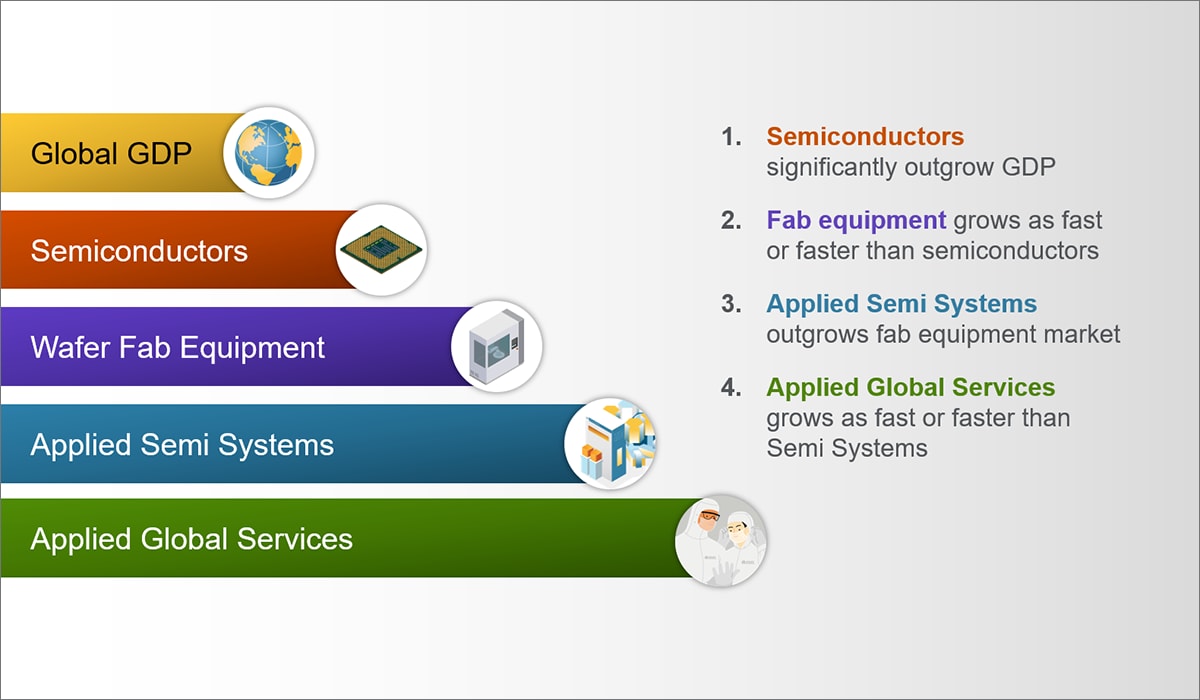
At Applied Materials’ 2021 investor meeting, we suggested that the semiconductor industry had transitioned into a fourth major era of computing. This new “IoT + AI” era began in 2018, when machines generated more data than humans for the first time, complementing the markets for PCs and smartphones that defined the second and third computing eras. Each era creates a new wave of growth by effectively doubling the size of the industry, putting us on track to reach $1 trillion by the end of the decade, as suggested by multiple third-party forecasts.
Power-Hungry AI Applications Demand More Energy-Efficient Computing
The computing industry’s relentless pursuit of more capable artificial intelligence is triggering the need for major inflections in logic and memory. While data center AI is expected to eclipse PCs and then smartphones as the number one driver of leading-edge foundry-logic and DRAM wafer starts, the growth of AI may be gated by the limits of the power grid – and push carbon neutrality goals years into the future – unless we dramatically improve the efficiency of chips and systems.
